Method of manufacturing a semiconductor device

a manufacturing method and semiconductor technology, applied in the direction of semiconductor devices, electrical devices, transistors, etc., can solve the problems of inability to control crystal orientation, limitation of tfts electrical characteristics, and dispersion of electrical characteristics

Inactive Publication Date: 2002-10-24
SEMICON ENERGY LAB CO LTD
View PDF79 Cites 66 Cited by
  • Summary
  • Abstract
  • Description
  • Claims
  • Application Information

AI Technical Summary

Problems solved by technology

However, it is impossible to control crystal orientation, so that its arrangement has an arbitrary direction, in crystalline semiconductor films formed by using heat treatment or laser annealing (a technique of crystallizing a semiconductor film by the irradiation of laser light) to crystallize an amorphous semiconductor film deposited by plasma CVD or LPCVD.
This becomes a source of limitations in the electrical characteristics of the TFTs.
This dispersion is a cause of dispersion in electrical characteristics and a factor in display irregularities if the crystalline semiconductor films are used as display portions of electronic equipment.
However, there is a problem with the aforementioned method in that an excessive amount of the metal element remains as a metal compound within high resistance regions (channel forming regions and offset regions).
This becomes a problem that can harm the stability of the TFT electrical characteristics as well as the reliability.

Method used


Image

  • Method of manufacturing a semiconductor device
  • Method of manufacturing a semiconductor device
  • Method of manufacturing a semiconductor device

Examples


embodiment 1

[0066] Embodiment 1

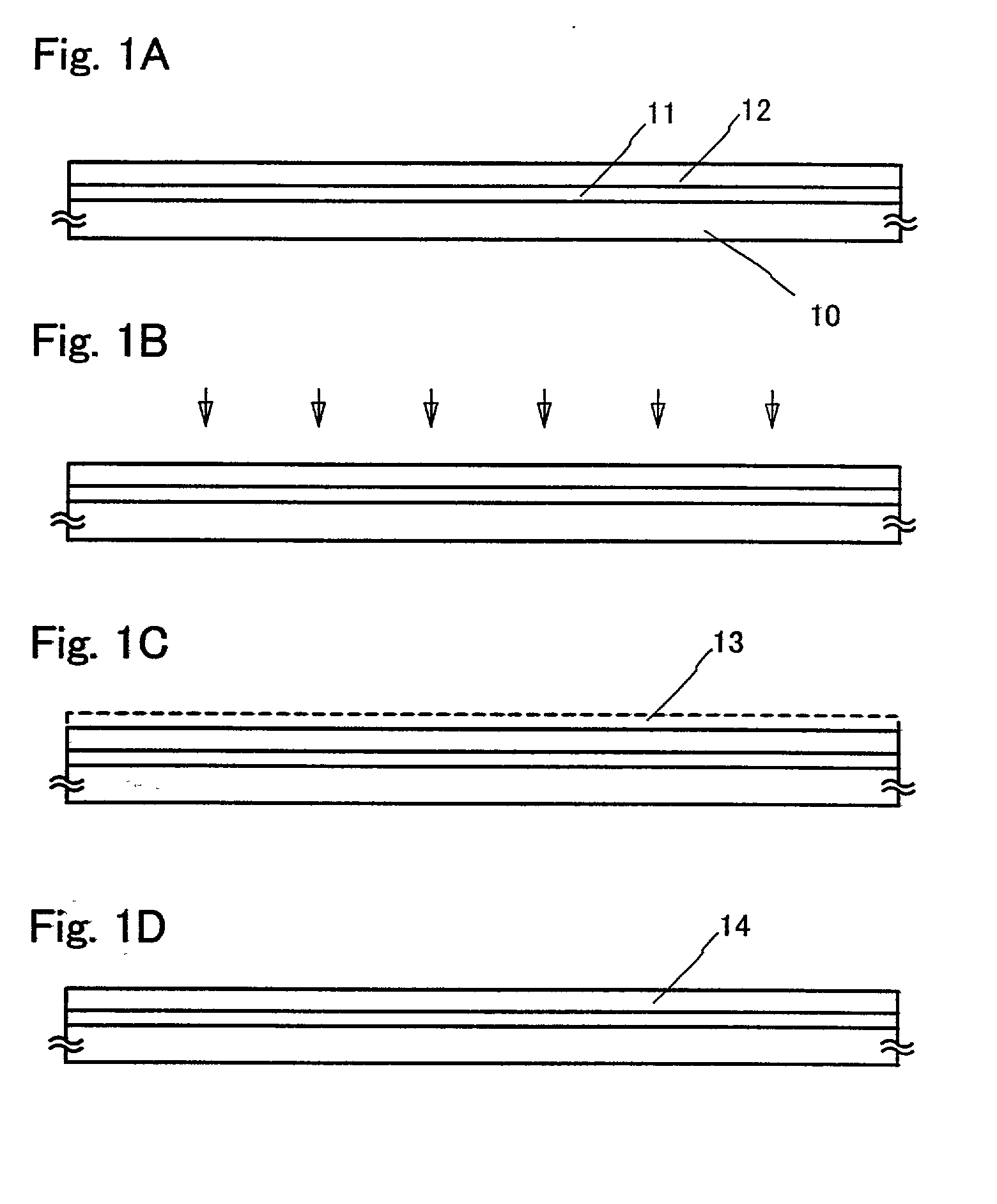
[0067] An embodiment of the present invention is explained using the cross sectional diagrams of FIGS. 1A to 1D.

[0068] A synthesized quartz glass substrate, and non-alkaline glass substrates such as barium borosilicate glass substrates and aluminum borosilicate glass substrates may be used for a substrate 10 in FIG. 1A. For example, Corning Corp. #7059 glass, #1737 glass, and the like can be applied preferably. Further, plastic substrates having heat resistant properties capable of withstanding the processing temperatures of this embodiment may also be used. A synthesized quartz glass substrate is applied in Embodiment 1.

[0069] A base insulating film 11 is formed by a known means (such as LPCVD or plasma CVD) on the substrate 10 from a film such as a silicon nitride film, a silicon oxynitride film, or a silicon oxide film. A 150 nm thick silicon oxynitride film (composition ratio: Si=32%, O=27%, N=24%, H=17%) is formed as the base insulating film in Embodiment 1.

[...

embodiment 2

[0076] Embodiment 2

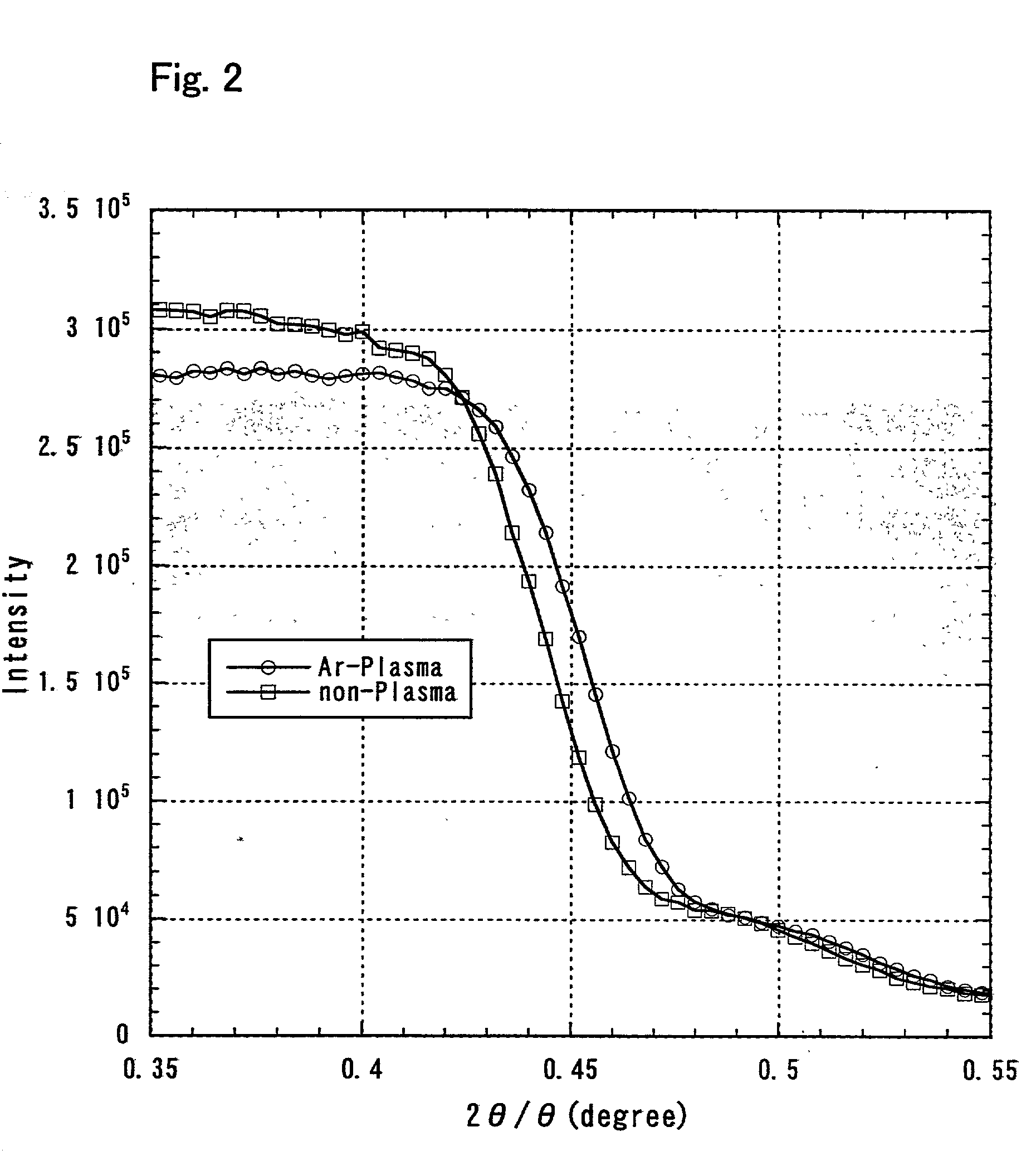
[0077] In order to verify the effectiveness of the present invention, an experiment was performed as discussed below using Ar from among elements capable of being used in making a plasma (such as inert gas elements and ammonia).

[0078] A synthesized quartz glass substrate was used as the substrate 10 in FIG. 1A, and an amorphous silicon film was formed to a film thickness of 65 nm on the substrate by using an LPCVD apparatus. Test pieces of this type were then either exposed to an atmosphere in which Ar had been made into a plasma, or were not exposed thereto. The exposure conditions for the Ar plasma atmosphere are a gas flow rate of 100 sccm, an RF power of 200 W, and a substrate temperature of 400.degree. C. in a plasma CVD apparatus.

[0079] An aqueous nickel acetate solution (per weight concentration 5 ppm, volume 10 ml) is next applied to the surface of the amorphous silicon film by spin coating, forming a metal containing layer, and heat treatment is performed...

embodiment 3

[0083] Embodiment 3

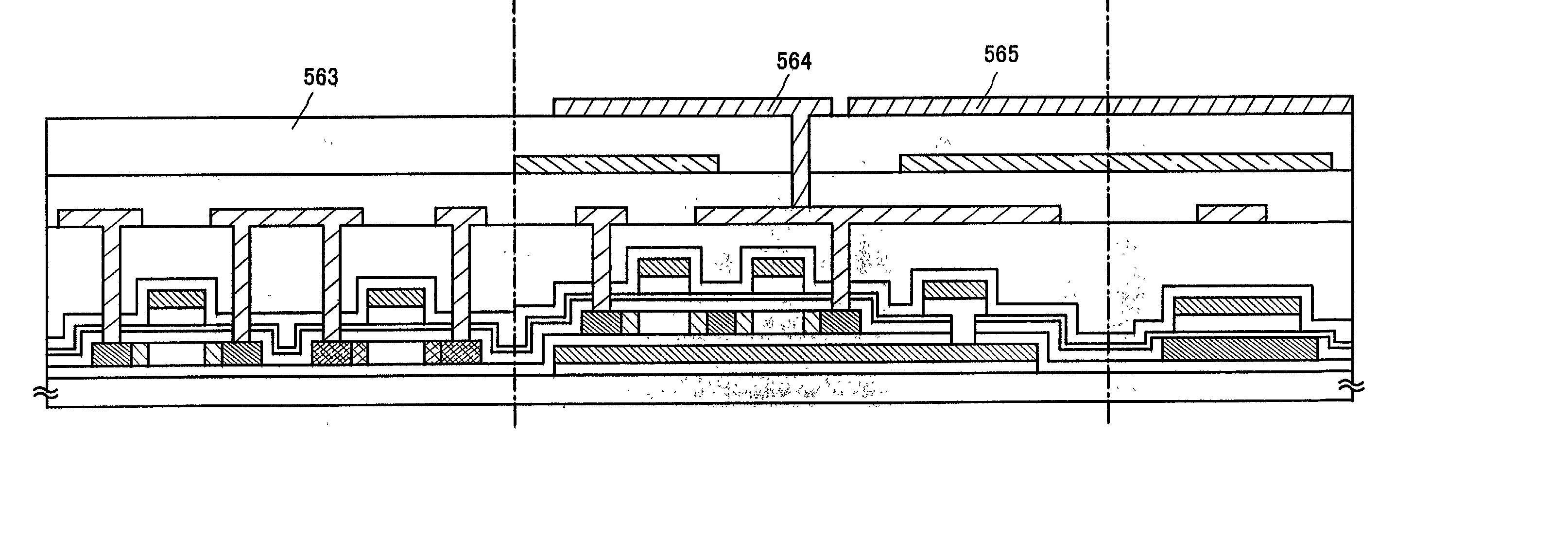
[0084] An embodiment of the present invention is explained on results obtained by measuring electrical characteristics of TFTs manufactured by using crystalline semiconductor films. One of the crystalline semiconductor film is crystallized before plasma processing is performed in accordance with Embodiment 2, and the other is crystallized without the plasma processing. Note that the TFTs are manufactured in the same manner as Embodiment 6 except for step of crystallizing.

[0085] FIG. 19A shows a probability statistical distribution diagram with respect to the S value and FIG. 19B shows a probability statistical distribution diagram with respect to the electric field effect mobility. N-channel TFTs with channel forming region lengths / widths 50 / 50 .mu.m are measured in FIGS. 19A and 19B. The axis of abscissas indicates the electrical characteristic and the axis of ordinates indicates the probability distribution in FIGS. 19A and 19B. The more the probability distribu...


PUM

PropertyMeasurementUnit
permissible deviation angleaaaaaaaaaa
temperatureaaaaaaaaaa
sizeaaaaaaaaaa

Abstract

The number of grains in active regions of devices can be made uniform by making the grains of crystalline semiconductor films, obtained by thermal crystallization using a metal element, smaller. The present invention is characterized in that a semiconductor film is exposed within an atmosphere in which a gas, having as its main constituent one or a plurality of members from the group consisting of inert gas elements, nitrogen, and ammonia, is processed into a plasma, and then thermal crystallization using a metal element is performed. The concentration of crystal nuclei1 generated is thus increased, making the grain size smaller, by performing these processes. Heat treatment may also be performed, of course, after exposing the semiconductor film, to which the metal element is added, to an atmosphere in which a gas, having as its main constituent one or a plurality of members from the group consisting of inert gas elements, nitrogen, and ammonia, is processed into a plasma.

Description

[0001] 1. Field of the Invention[0002] The present invention relates to a method of manufacturing a semiconductor device having circuits formed by thin film transistors (hereafter referred to as TFTs). For example, the present invention relates to electro-optical devices, typically liquid crystal display devices, and to electronic equipment in which electro-optical devices are installed as parts. Further, the present invention relates to a method of manufacturing such devices. Note that the term semiconductor device in this specification indicates a category of general devices capable of functioning by utilizing semiconductor characteristics, and the above-mentioned electro-optical devices and electronic equipment are also included in the category of semiconductor devices.[0003] 2. Description of the Related Art[0004] Research is widespread into techniques of forming crystalline semiconductor films, and increasing crystallinity, by performing heat treatment, laser annealing, or both...

Claims


Application Information

Patent Timeline
Patent Type & Authority Applications(United States)
IPC IPC(8): H01L21/336H01L21/77H01L21/84H01L27/12H01L29/786
CPCH01L27/12H01L29/66757H01L29/78621H01L27/1277H01L29/78675H01L29/78648H01L29/78645
Inventor MITSUKI, TORUSHICHI, TAKESHIMAEKAWA, SHINJISHIBATA, HIROSHIMIYANAGA, AKIHARU
Owner SEMICON ENERGY LAB CO LTD
Why Eureka
Try Eureka