Charge separation type heterojunction structure and manufacturing method therefor

a technology of heterojunction structure and manufacturing method, which is applied in the direction of physical/chemical process catalysts, fullerenes, natural mineral layered products, etc., can solve the problems of deterioration in structure, adverse effects of electronic properties, and fragile strength of evaporated films produced therefrom, so as to improve durability and electronic physical properties.

Inactive Publication Date: 2003-07-10
SONY CORP +1
View PDF0 Cites 19 Cited by
  • Summary
  • Abstract
  • Description
  • Claims
  • Application Information

AI Technical Summary

Benefits of technology

[0044] It is therefore an object of the present invention to provide a charge separation type heterojunction structure in which, by establishing a method for non-destructively identifying a fullerene polymer film and by applying the polymer film to a layered structure, it is possible to produce a solar cell etc which is improved not only in durability and electronic physical properties but also in various physical properties.

Problems solved by technology

However, the molecules of fullerene forms, such as C.sub.60 or C.sub.70, the most mass-producible, are of zero dipole moment, such that evaporated films produced therefrom are fragile in strength, because only the van der Waal's force acts between its molecules.
Thus, if the evaporated film is exposed to air, molecules of oxygen or water tend to be diffused and intruded into the gap between the fullerene molecules (FIG. 2), as a result of which the evaporated film is not only deteriorated in structure but adverse effects may be occasionally produced in its electronicproperties.
This fragility of the fullerene poses a problem in reference to device stability when applying the fullerene to fabrication of a thin-film electronic device.
In these methods, in which light is illuminated on a previously formed evaporated fullerene film, numerous cracks tend to be formed in the film surface due to volumetric contraction produced on polymerization, so that produced films are problematic in strength.
Moreover, it is extremely difficult to form a uniform thin film of a large surface area.
It has also been known to apply pressure or heat to fullerene molecules or to cause collision of fullerene molecules against one another.
However, lacking the solvent capable of dissolving the fullerene polymer, it is difficult to directly evaluate the actual molecular weight distribution of the polymer.
Even with the mass evaluation by Laser Desorption Ionization Time-of-Fight Mass Spectroscopy (LDITOF-MS), it is difficult to make correct evaluation of the mass distribution of an actual fullerene polymer due to the absence of suitable solvents or to the reaction taking place between C.sub.60 and the matrix molecule.
However, the polymerization between C.sub.70 molecules is more difficult to understand than in that between C.sub.60.
However, the solar cells, hitherto proposed, are common in exploiting the fullerene evaporated film, so that the above-mentioned problem attributable to the fragility of the evaporated film, in particular the durability or physical properties of electrons, as yet remains unsolved.
However, it has scarcely been attempted up to now to use the material as a constituent material for fabrication of the solar cells.
In addition, the fact that the method of definitely identifying the fullerene polymer film by a non-destructive technique has not been established possibly needs to be taken into consideration.
However, insofar as carbonaceous thin film, such as a fullerene polymer film, is concerned, difficulties are encountered in measurement due to failure in definite observation of the pattern of free induction attenuation depending on electrical conductivity and to transverse relaxation to nuclear spin by dangling unpaired spin.
Moreover, the nuclear magnetic resonance method is not suited as means for monitoring structural changes in the carbonaceous thin film material due to difficulties encountered in magic angle spin of an individual sample.

Method used


Image

  • Charge separation type heterojunction structure and manufacturing method therefor
  • Charge separation type heterojunction structure and manufacturing method therefor
  • Charge separation type heterojunction structure and manufacturing method therefor

Examples


example 2

Formation of Polythiophene Thin Film (Electrically Conductive Organic Film) and Measurement of Physical Properties Thereof)

[0239] On this ITO film was then formed a commercial polythiophene thin film having a sulfur radical as a dopant. The measured results of the PES of this polythiophene thin film are shown in FIG. 45.

[0240] It was seen from the above results that the valence band edge level of the polythiophene thin film exists at 4.82 eV below vacuum.

[0241] Moreover, a polythiophene thin film was also formed on the quartz glass and measurement was made of the current-voltage characteristics thereof. FIG. 46 shows the measured results of the V-I characteristics and absorption coefficients by the light quantum energy.

[0242] A polythiophene thin film was formed on each of an ITO thin film and on a metal film. First, the Fermi level of the ITO and gold was measured by the photoelectron emission method and, based on the measured value, the Fermi level of the polythiophene thin film w...

example 3

Formation of a Fullerene Polymer Film and Measurement of Various Physical Properties

[0244] A fullerene polymer film then was formed on the above-mentioned polythiophene thin film.

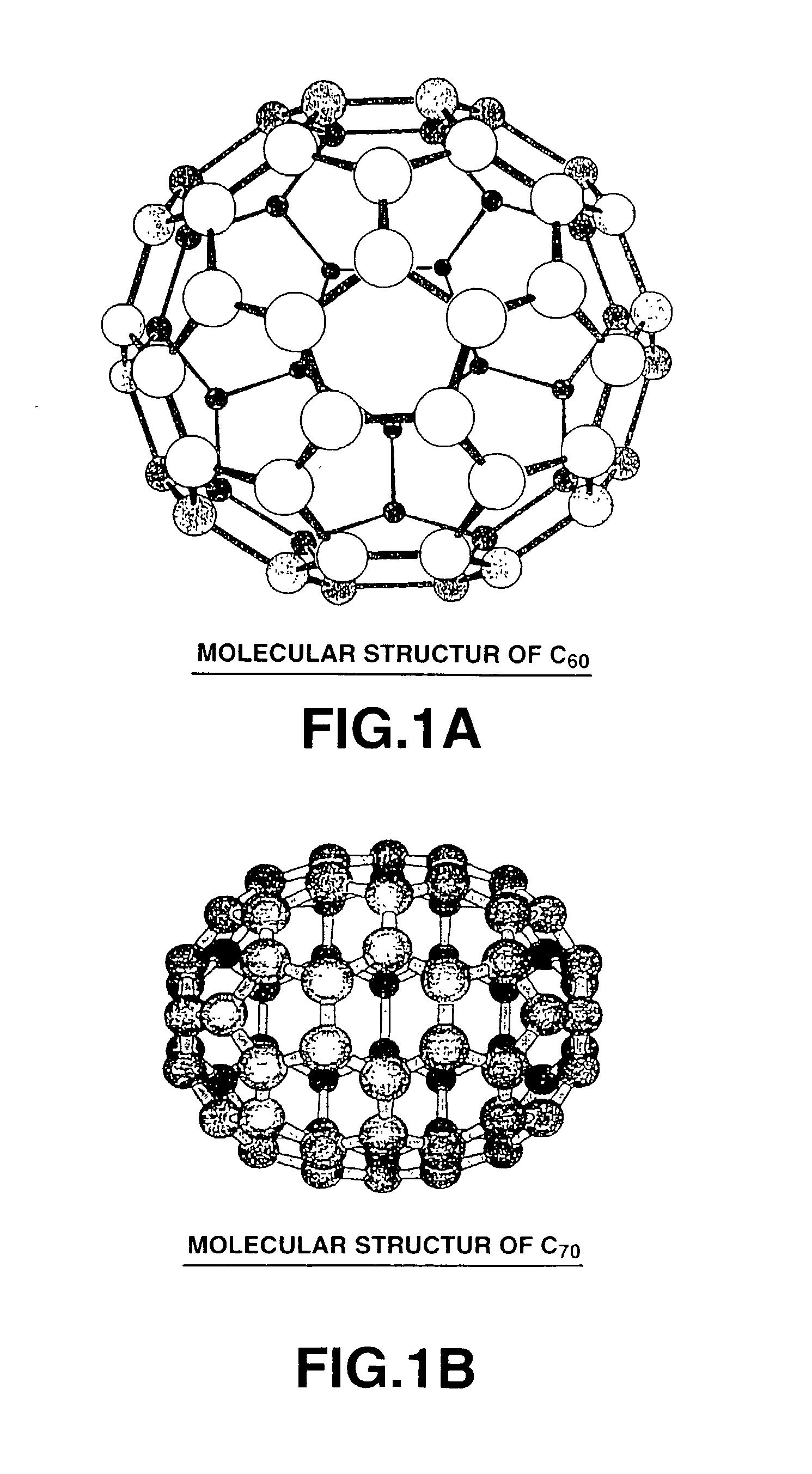
[0245] First, fullerene molecules, as a starting material, was prepared in the following manner. In an apparatus shown in FIG. 35, arc discharge was effected by the 150 A direct current in an atmosphere of 100 Torr of helium, using a graphite rod 35 cm in length as a positive electrode. After fullerene was substantially vaporized to produce the fullerene containing soot, the polarities of the two electrodes were reversed and deposited heaped on the inherent negative electrode, such as carbon nanotubes, were further vaporized to produce the soot. The soot heaped in a water-cooled reaction vessel was recovered by a sweeper to produce crude fullerene by extraction with toluene. This crude fullerene was washed with hexane, dried and purified by sublimation in vacuum. The fullerene molecules, thus produced, were...

example 4

Manufacture of Heterojunction Structure and its Physical Properties

[0288] On the above-mentioned layered structure, including a polythiophene film and a C60 polymer film, deposited on an ITO electrode, an aluminum electrode was formed as a counter-electrode in the following manner. First, the inside of a vapor deposition device was evacuated to vacuum of 10.sup.-8 Torr by a turbo-pump and subsequently back-filled with a high purity hydrogen gas. An aluminum film then was formed on the C.sub.60 polymer film of the layered structure in a hydrogen atmosphere of 10.sup.-5 Torr to produce a heterojunction structure.

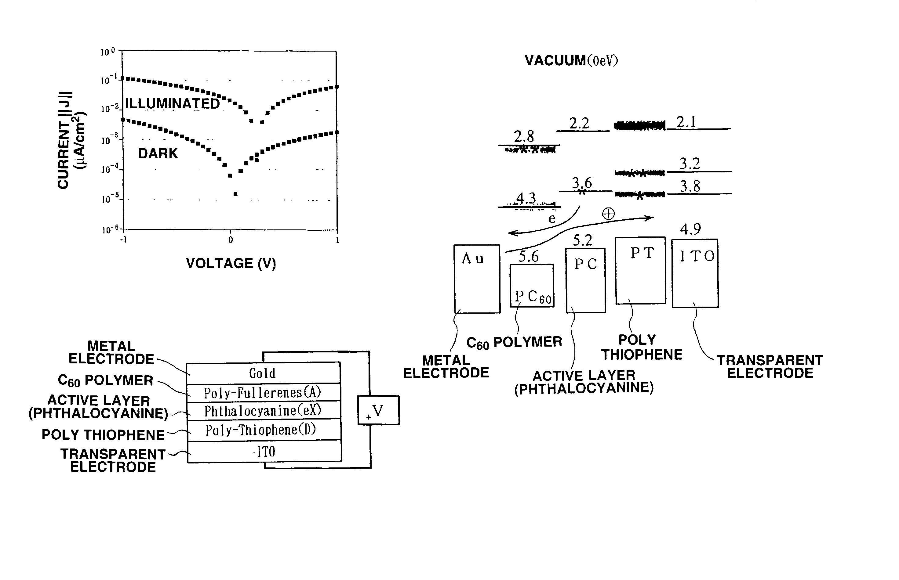
[0289] From the evaluation of the valence electron band by the photoelectron emission method, Fermi level by the contact potential difference method and the band gap by the optical technique, the band structure of the produced heterojunction structure is as shown in FIG. 55.

[0290] The V-I characteristics of the heterojunction structure were evaluated. The results are shown in ...


PUM

PropertyMeasurementUnit
band gapaaaaaaaaaa
electrical resistivityaaaaaaaaaa
band gapaaaaaaaaaa

Abstract

A charge separation heterojunction structure which uses a fullerene polymer film as a part of its constituent materials and which may be used to produce a solar cellor a light emitting diode superior in durability, physical properties of electrons and economic merits. The heterojunction structure is such a structure in which an electron-donating electrically conductive high-polymer film and an electron-accepting fullerene polymer film are layered between a pair of electrodes at least one of which is light transmitting. In forming the layers, the fullerene polymer film is identified using in particular the Raman and Nexafs methods in combination so that upper layers are formed after identifying the polymer film.

Description

[0001] 1. Field of the Invention[0002] This invention relates to a charge separation type heterojunction structure used in e.g., a solar cell or a light emitting diode and which has fullerene as a portion of a constituting material thereof. This invention also relates to a manufacturing method for the charge separation type heterojunction structure.[0003] 2. Description of Prior Art[0004] Up to now, a silicon pn junction semiconductor etc has been extensively used in e.g., a solar cell or a light emitting diode. Of late, the energy conversion efficiency of the silicon pn junction semiconductor has been improved appreciably in comparison with that when the silicon pn junction semiconductor was initially devised.[0005] Among the materials for the solar cell, there is e.g., titania in addition to silicon. Recently, however, fullerene, as a carbon compound, has attracted attention. The features of fullerene is hereinafter explained in connection with the discovery and the history of dev...

Claims


Application Information

Patent Timeline
Patent Type & Authority Applications(United States)
IPC IPC(8): B01J35/00C01B31/02H01L21/302H01L21/461H01L51/00H01L51/30H01L51/40H01L51/42H01L51/50
CPCB01J35/002Y02E10/549B82Y10/00B82Y30/00B82Y40/00C01B31/02C01B31/0206C01B31/0213H01L51/0002H01L51/0006H01L51/0034H01L51/0035H01L51/0036H01L51/0038H01L51/0039H01L51/0046H01L51/0047H01L51/0078H01L51/42H01L51/424H01L51/4246H01L51/5012H01L2251/308Y10S977/932B01J35/004C01B32/05C01B32/15Y10T428/31924C01B32/156H10K71/10H10K71/125H10K85/10H10K85/113H10K85/111H10K85/115H10K85/114H10K85/211H10K85/215H10K85/311H10K30/00H10K30/211H10K30/20H10K50/11H10K2102/103
Inventor RAMM, MATTHIASATA, MASAFUMI
Owner SONY CORP
Why Eureka
Try Eureka