

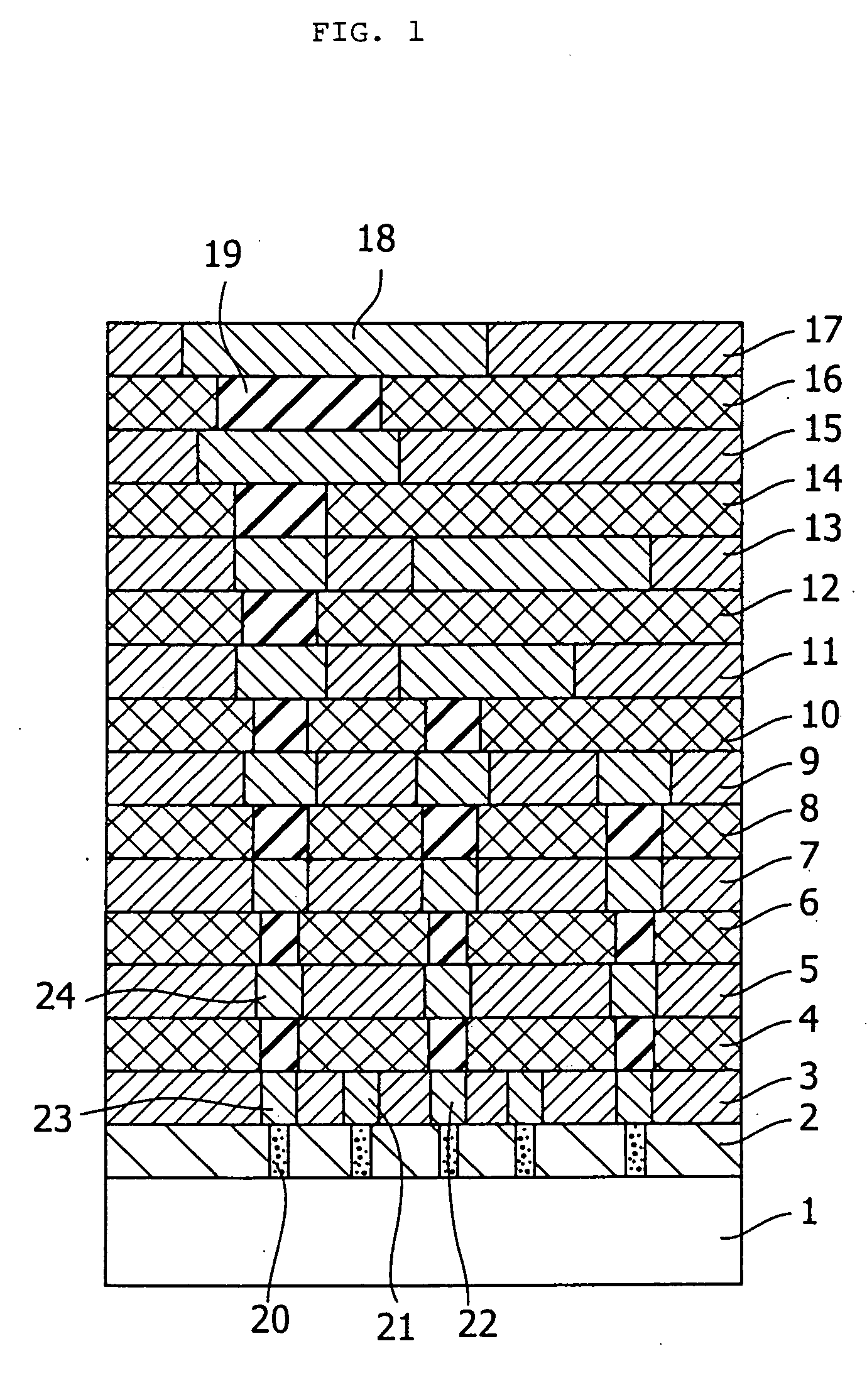
Composition for forming porous film, porous film and method for forming the same, interlevel insulator film, and semiconductor device
a technology of porous film and hygroscopic properties, applied in the direction of solid-state devices, inorganic chemistry, building components, etc., can solve the problems of increasing the delay time of interconnection, hindering the enhancement of the performance of semiconductor circuits, and increasing the cost of synthesis of siloxane polymer precursor solutions, so as to improve the mechanical strength of the semiconductor device, improve the mechanical properties, and improve the mechanical properties. the effect of good mechanical properties
- Summary
- Abstract
- Description
- Claims
- Application Information
AI Technical Summary
Benefits of technology
Problems solved by technology
Method used
Image

Examples
synthetic example 2
[0069] (Synthesis of Siloxane Polymer with Basic Catalyst)
[0070] A solution of tetraethoxysilane (60 g) and methyltrimethoxysilane (30 g) was added to the mixture of the solution of an aqueous 40wt % methylamine solution (log), ultra pure water (640 g) and ethanol (1200 g), and stirred for four hours at 75.degree. C. The ethanolic solution of the silicone polymer was obtained.
synthesis example 3
[0071] (Synthesis of Siloxane Polymer with Basic Catalyst)
[0072] A solution of tetramethoxysilane (40 g) and methyltrimethoxysilane (30 g) was added to the mixture of an aqueous 28wt % ammonia solution (10 g), ultra pure water (640 g) and ethanol (1200 g), and stirred for four hours at 75.degree. C. The ethanolic solution of silicone polymer was obtained.
example 1
[0073] An aqueous 5wt % tetramethylammonium caproate solution (90 g) and propylene glycol monopropyl ether (700 g) were added at 25.degree. C. to the siloxane polymer solution (650 g) obtained in Synthetic Example 1. After stirring for one hour, the reaction mixture was concentrated under reduced pressure at 40.degree. C. so that the coating liquid (700 g) was obtained. Then, it was applied on an eight-inch wafer with a spin coater for one minute at 1,500 rpm. The film thickness, when heated for two minutes at 120.degree. C. using a hot plate, was 8,000A. After it was further heated at 250.degree. C. for three minutes, it was heated at 450.degree. C. for one hour in a nitrogen atmosphere in a clean oven. The thickness was 7,200A. The dielectric constant of the obtained film was 2.2 and the modulus of elasticity thereof was 6.5 Gpa. The coating liquid obtained was left stand at 23.degree. C. for 30 days. Afterwards, the film was obtained in the same manner as the above. Then, the val...
PUM
| Property | Measurement | Unit |
|---|---|---|
| relative permittivity | aaaaa | aaaaa |
| relative permittivity | aaaaa | aaaaa |
| pore diameter | aaaaa | aaaaa |
Abstract
Description
Claims
Application Information