Group III-nitride based resonant cavity light emitting devices fabricated on single crystal gallium nitride substrates

a gallium nitride and resonant cavity technology, applied in the field of lighting arts, can solve problems such as difficult to fabricate reliable resonant cavity devices, loss of efficiency by stokes shift, reflective or light-scattering loss, and device failures associated with phosphor packaging, and achieve the problem of large volume and high-quality gallium nitride boule growth

Active Publication Date: 2005-04-28
SLT TECH
View PDF33 Cites 216 Cited by
  • Summary
  • Abstract
  • Description
  • Claims
  • Application Information

AI Technical Summary

Benefits of technology

[0013] According to one aspect, a method is provided for producing a resonant cavity light emitting device. A seed gallium nitride crystal and a source material are arranged in a nitrogen-containing superheated fluid that provides a medium for mass transport of gallium nitride precursors between the seed gallium nitride crystal and the source material. A surface of the seed gallium nitride crystal is prepared. The preparing includes applying a first thermal profile between the seed gallium nitride crystal and the source material while the seed gallium nitride crystal and the source material are arranged in the nitrogen-containing superheated fluid. Gallium nitride material is grown on the prepared surface of the seed gallium nitride crystal. The growing includes applying a second thermal profile which is different from the first thermal profile between the seed gallium nitride crystal and the source material while the seed gallium nitride crystal and the source material are arranged in the nitrogen-containing superheated fluid. Said growing produces a single-crystal gallium nitride substrate. A stack of group III-nitride layers are deposited on the single-crystal gallium nitride substrate. The stack includes a first mirror sub-stack and an active region adapted for fabrication into one or more resonant cavity light emitting devices.

Problems solved by technology

One of the major challenges with solid state lighting at present is efficient extraction of light from the light emitting diode.
Another challenge is that light emitting diodes typically emit only one wavelength, whereas for many applications at least one additional wavelength or white light would be desirable.
The use of phosphors, typically in a polymer matrix, allows generation of additional wavelengths and / or white light, but often entails loss of efficiency by Stokes shifts, reflective or light-scattering losses, and device failures associated with the phosphor packaging.
Resonant cavity devices offer a way to provide more efficient light extraction, but it has so far been difficult to fabricate reliable resonant cavity devices in the group III-nitride material system.
In spite of these well-known advantages, commercial group III-nitride light emitting devices generally continue to be grown heteroepitaxially on sapphire or silicon carbide substrates due to a lack of high quality large-area gallium nitride substrates.
The chemical passivity of nitrogen, a high melting temperature of gallium nitride, and other factors have heretofore made growth of large volume and high quality gallium nitride boules problematic.
The high n-type background causes substantial crystal opacity, for example optical absorption coefficients of around 200 cm−1 in the visible range, which is problematic for flip-chip light emitters, and causes the lattice constant to increase by about 0.01-0.02%, generating strain in epitaxial GaN layers deposited thereupon.
The undoped GaN substrates formed by this method have a rather limited carrier mobility, about 30-90 cm2 / V-s, which may be problematic in high-power devices.
Repeated application of epitaxial lateral overgrowth is not expected to substantially suppress the tilt boundaries.
Thus, epitaxial lateral overgrowth is not upwardly scalable in the lateral wafer dimension, and usable growth dimensions are limited to about the order of the spacings of the nucleation openings.
Furthermore, ELO does not produce a three-dimensional single-crystal boule, and the processing involved in producing each ELO gallium nitride wafer is labor-intensive, making automation of the ELO wafer formation process difficult.
However, these references focus on thin GaN epitaxial layers rather than bulk crystals and do not relate to resonant cavity devices.
However, the disclosed laser structure employs only a single cavity and has no capability for directional emission of two or more visible wavelengths of light or of white light.

Method used


Image

  • Group III-nitride based resonant cavity light emitting devices fabricated on single crystal gallium nitride substrates
  • Group III-nitride based resonant cavity light emitting devices fabricated on single crystal gallium nitride substrates
  • Group III-nitride based resonant cavity light emitting devices fabricated on single crystal gallium nitride substrates

Examples


Embodiment Construction

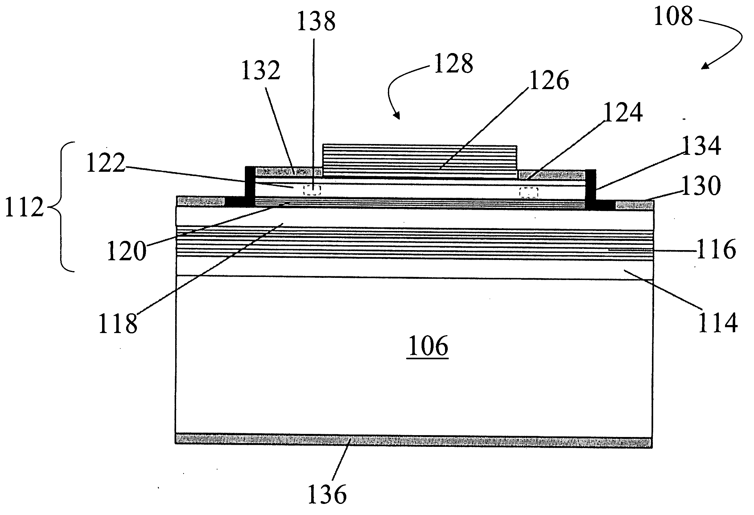
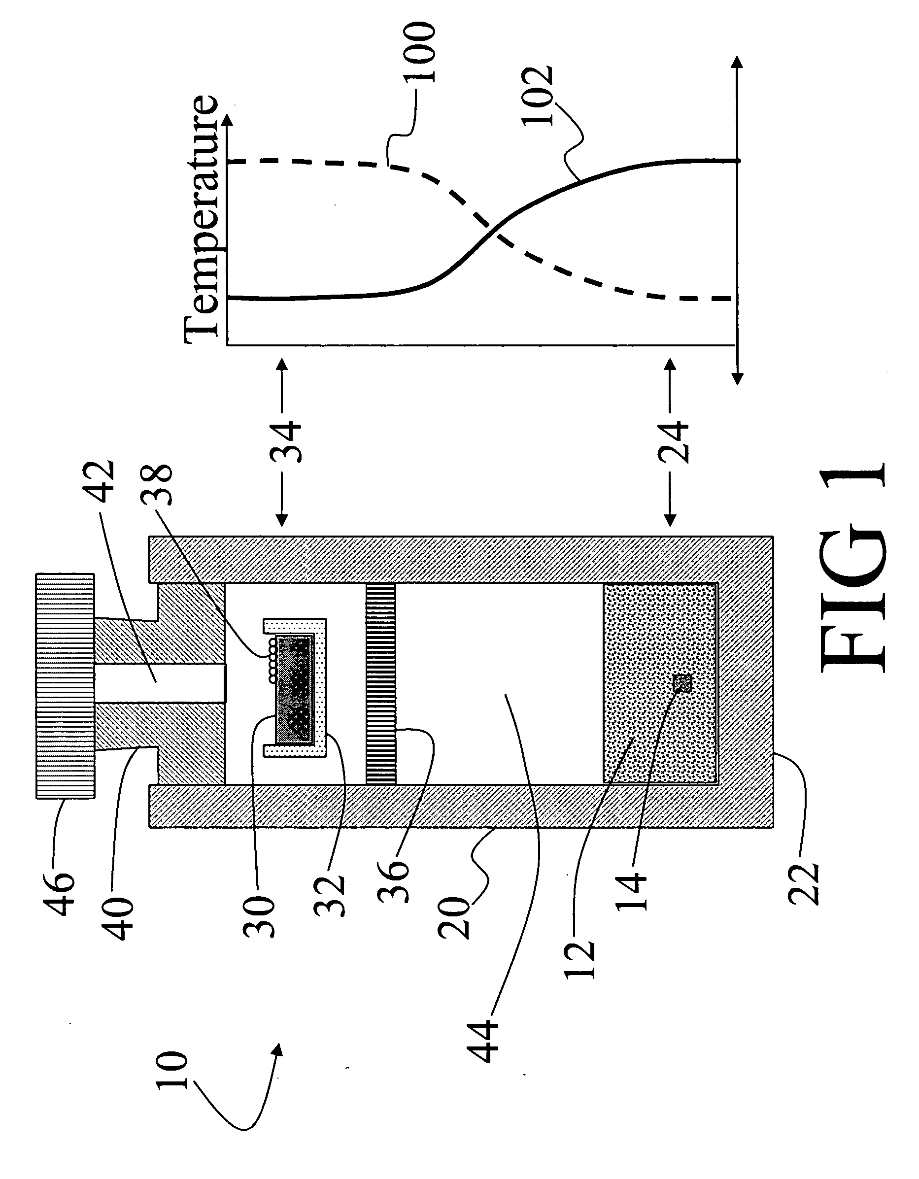
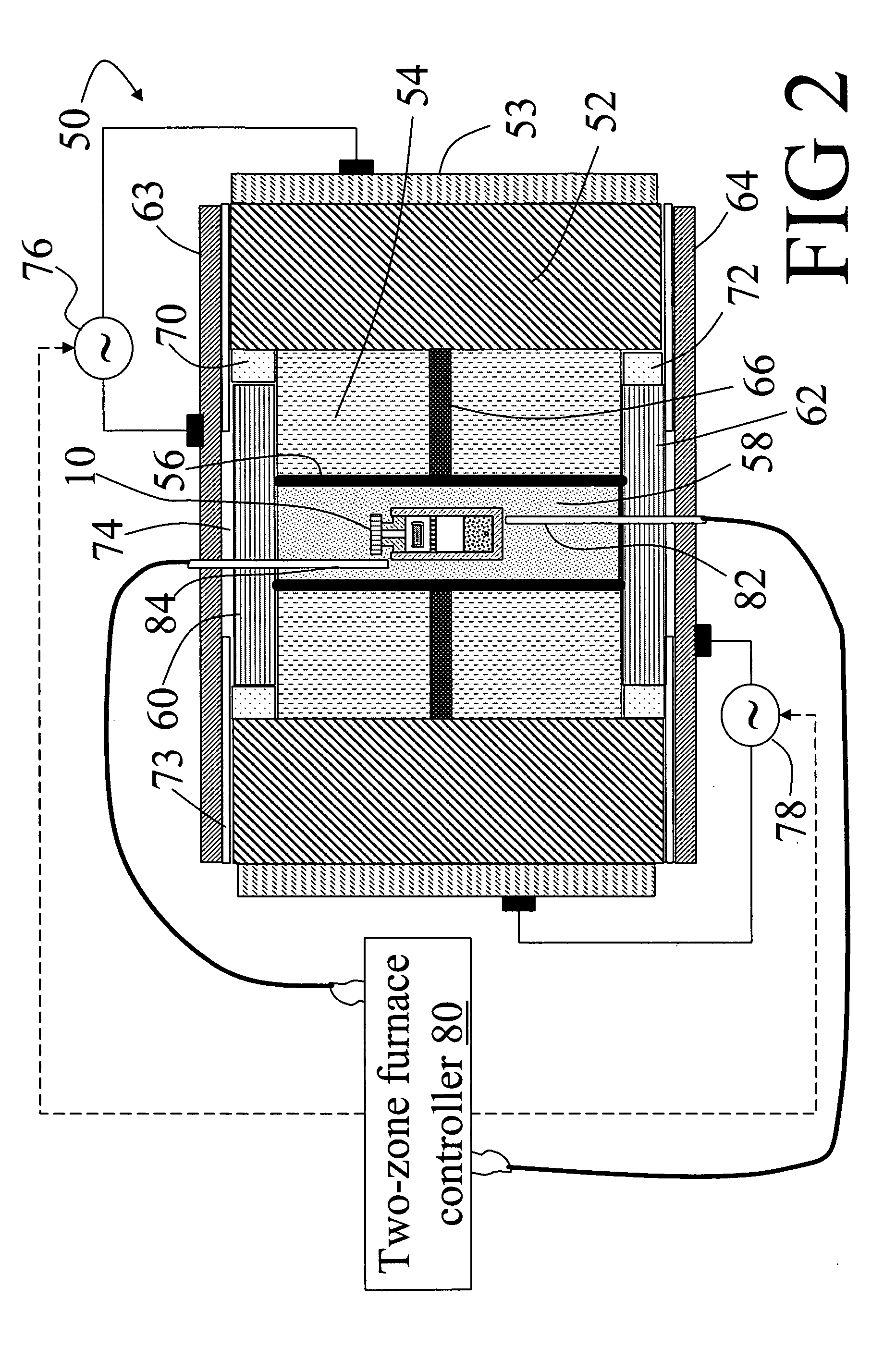
[0036] With reference to FIG. 1, a cell or capsule 10 is used in growing a three-dimensional gallium nitride boule 12 from a gallium nitride seed 14 using a recrystallization technique performed in a nitrogen-containing superheated fluid. The capsule 10 includes a main container 20 which is preferably generally cylindrical in shape with a diameter of about one inch or larger, although containers having other shapes and sizes are also contemplated. The container 20 includes a sealed bottom section 22, which is preferably integrally formed with the main container 20, although a separately formed bottom section that is welded or otherwise secured to the main container is also contemplated.

[0037] The container 20 including the bottom section 22 is preferably formed of at least one of copper, a copper-based alloy, gold, silver, palladium, platinum, iridium, ruthenium, rhodium, osmium, titanium, vanadium, chromium, iron, an iron-based alloy, nickel, a nickel-based alloy, zirconium, niobi...


PUM

PropertyMeasurementUnit
optical absorption coefficientaaaaaaaaaa
optical absorption coefficientsaaaaaaaaaa
thicknessaaaaaaaaaa

Abstract

In a method for producing a resonant cavity light emitting device, a seed gallium nitride crystal (14) and a source material (30) are arranged in a nitrogen-containing superheated fluid (44) disposed in a sealed container (10) disposed in a multiple-zone furnace (50). Gallium nitride material is grown on the seed gallium nitride crystal (14) to produce a single-crystal gallium nitride substrate (106, 106′). Said growing includes applying a temporally varying thermal gradient (100, 100′, 102, 102′) between the seed gallium nitride crystal (14) and the source material (30) to produce an increasing growth rate during at least a portion of the growing. A stack of group III-nitride layers (112) is deposited on the single-crystal gallium nitride substrate (106, 106′), including a first mirror sub-stack (116) and an active region (120) adapted for fabrication into one or more resonant cavity light emitting devices (108, 150, 160, 170, 180).

Description

BACKGROUND [0001] The present invention relates to the lighting arts. It especially relates to resonant cavity light emitting devices such as resonant cavity light emitting diodes (RCLED's) and vertical cavity surface emitting lasers (VCSEL's), and will be described with particular reference thereto. However, the invention will also find application in conjunction with other group III-nitride based light sources. [0002] One of the major challenges with solid state lighting at present is efficient extraction of light from the light emitting diode. Another challenge is that light emitting diodes typically emit only one wavelength, whereas for many applications at least one additional wavelength or white light would be desirable. The use of phosphors, typically in a polymer matrix, allows generation of additional wavelengths and / or white light, but often entails loss of efficiency by Stokes shifts, reflective or light-scattering losses, and device failures associated with the phosphor ...

Claims


Application Information

Patent Timeline
Patent Type & Authority Applications(United States)
IPC IPC(8): C30B9/00H01L33/00H01L33/10
CPCC30B9/00C30B29/403Y10T117/1064H01L33/007H01L33/105C30B29/406H01S5/187H01S5/323
Inventor D'EVELYN, MARK PHILIPCAO, XIAN-ANZHANG, ANPINGLEBOEUF, STEVEN FRANCISHONG, HUICONGPARK, DONG-SILNARANG, KRISTI JEAN
Owner SLT TECH
Why Eureka
Try Eureka