Silicon nitride film and semiconductor device, and manufacturing method thereof

a technology of silicon nitride and semiconductors, applied in vacuum evaporation coatings, coatings, chemistry apparatuses and processes, etc., can solve the problems of film damage, insufficient characteristic of desired shape and reliability, and inability to divert manufacturing techniques developed in a large-scale integrated circui

Inactive Publication Date: 2005-05-19
SEMICON ENERGY LAB CO LTD
View PDF56 Cites 7 Cited by
  • Summary
  • Abstract
  • Description
  • Claims
  • Application Information

AI Technical Summary

Benefits of technology

[0008] A silicon nitride film that is cure and does not penetrate alkali ion can be formed with decompression CVD method; however, film formation temperature of more than 750° C. was necessary. Film can be formed with plasma CVD method; however, there were problem such as film was damaged due to charged particle in the plasma, and likely to have defect and pinhole. Furthermore, under film formation temperature of 500° C. or less, hydrogen is contained in the film, which decreased the stability of film. Regarding this, insulator target of silicon nitride and the like can be also used with high-frequency sputtering method, and silicon nitride film without a contamination of hydrogen into the film can be formed. However, the method was known to have a large compressive stress in general, which peeling of the film was sometimes a problem.
[0011] The present invention has been made in view of the problems mentioned above. An object of the present invention is to apply an insulating film of cure and high quality that is suitably applicable as gate insulating film and protective film to a technique that the insulating film is formed at the glass substrate under a temperature of strain point or lower, and to a semiconductor device realizing high efficiency and high reliability by using it.
[0014] The present invention contains hydrogen with the concentration of 1×10²¹ / cm3 or less, oxygen with the concentration of from 5×10¹⁸ to 5×10²¹ / cm3, and furthermore, provides the silicon nitride film having the characteristic of having an etching rate of 10 nm / min or less with respect to mixed solution containing an ammonium hydrogen fluoride (NH4HF2) of 7.13% and an ammonium fluoride (NH4F) of 15.4%. The silicon nitride film having such hydrogen and oxygen content and the etching characteristic exists in semiconductor device, and not only as the region where electrical insulation such as gate insulating film and dielectric protective film of capacitor portion is required, but can be also applied as the protective film that diffusion of the gas and ionic impurity is prevented.
[0018] By having such hydrogen and oxygen content, and the etching characteristic, in applying into the gate insulating film, a gate leak current can be decreased, electric field effect mobility, subthreshold coefficient, conductance (gm), and the like can be in a good condition, the long-term change of the transistor characteristic in the continuous operation can be decreased, and production yield and disorder in characteristics can be improved. Furthermore, by intervening silicon oxide film between crystalline semiconductor film and silicon nitride film, such effect can be exerted more effectively.

Problems solved by technology

Forming a polycrystalline silicon film on an insulating film such as glass and quartz and in the case realizing an integrated circuit using it, it was impossible to divert manufacturing technique itself developed in a large-scale integrated circuit.
It was not only the problem of crystalline of the polycrystalline silicon film, but also an insulating film conventionally manufactured by various methods and a semiconductor element using it could not exert enough characteristic of desired shape and reliability at present.
Film can be formed with plasma CVD method; however, there were problem such as film was damaged due to charged particle in the plasma, and likely to have defect and pinhole.
Furthermore, under film formation temperature of 500° C. or less, hydrogen is contained in the film, which decreased the stability of film.
However, the method was known to have a large compressive stress in general, which peeling of the film was sometimes a problem.
Moreover, in a gate insulating film of TFT formed by depositing the insulating film, an interface level concentration is consequently increased; therefore, a good interface could not be formed.
In addition, also from the cleanliness of the interface, it was problem that the polycrystalline silicon film formed on the insulating substrate is likely to be contaminated.
In particular, chemical pollution was difficult to identify the cause of pollution and pollutant pathway clearly.
Therefore, boron contamination which source is considerable to be filter material of clean room, and phosphorus and organic matter contamination from wall material and sealing material, and the like are difficult to prevent only in daily substrate management; therefore, the more the size of the glass substrate is grown, the more difficult it becomes.
As described above, Cu wiring is formed with damascene structure which the wiring is buried in the insulating film; however, without using an appropriate barrier film, there is a problem that the wiring can be easily diffused into the insulating film and layered interface of surrounding.

Method used


Image

  • Silicon nitride film and semiconductor device, and manufacturing method thereof
  • Silicon nitride film and semiconductor device, and manufacturing method thereof
  • Silicon nitride film and semiconductor device, and manufacturing method thereof

Examples


embodiment 1

[0076] For the substrate applicable at the present embodiment, a glass substrate which material is barium borosilicate glass, alumino borosilicate glass, aluminum silicate glass, and the like are suitable. Typically, a glass substrate 1737 produced by Corning Co. (strain point of 667° C.), AN100 produced by Asahi Glass Co. (strain point of 670° C.), and the like are applicable; however, it should be noted that there is no particular limit as long as other similar substrates. In either case, a glass substrate with strain point of 700° C. or less is applicable in the present invention. The present embodiment gives description concerning one embodiment that forms Micro Processor Unit (MPU) using the silicon nitride film manufactured with high-frequency magnetron sputtering method on the glass substrate with strain point of 700° C. or less.

[0077] Note that, in the present invention, the substrate with strain point of 700° C. or higher is not excluded. Needless to say, a synthesized qua...

embodiment 2

[0098] In Embodiment 1, after the crystalline silicon film shown in FIG. 10(B) is obtained, as shown in FIG. 11, YAG laser, YVO4 laser, and YLF laser can be used as solid state laser of continuous oscillation type. Second higher harmonic wave of YAG laser, YVO4 laser, and YLF laser is radiated. For example, second higher harmonic wave (532 nm) of YVO4 laser is concentrated into a linear shape, scanned at the speed of from 1 to 100 cm / sec to improve crystalline. Crystalline silicon film having smooth surface can be obtained by using continuous oscillation laser in the step, and can be set the maximal value of uneven shape of the surface to 10 nm or less, preferably 5 nm or less.

embodiment 3

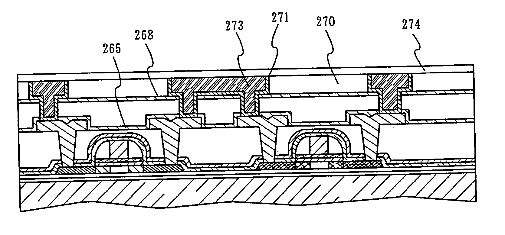
[0099] In the present embodiment, the structure of gate electrode is differed, and the structure of semiconductor device much appropriated to configurations is described referring to the drawings. It should be noted that the silicon nitride film on the present invention is also applied in each region of the semiconductor device.

[0100] In FIG. 13(A), the semiconductor films from 216 to 218 are formed as same as Embodiment 1. In gate insulating film 240, silicon nitride film manufactured by high-frequency magnetron sputtering method with a thickness of from 10 to 80 nm is applied; however, in the interface with semiconductor, silicon oxide film with a thickness of from 1 to 5 nm formed by sputtering or an oxidation plasma treatment is intervened. Accordingly, this can prevent from increasing interface level concentration by contacting silicon nitride film and semiconductor film directly, and the damage during film formation can be decreased.

[0101] Gate electrodes 243, 244 and capaci...


PUM

PropertyMeasurementUnit
thicknessaaaaaaaaaa
thicknessaaaaaaaaaa
thicknessaaaaaaaaaa

Abstract

An object of the present invention is to apply an insulating film of cure and high quality that is suitably applicable as gate insulating film and protective film to a technique that the insulating film is formed on the glass substrate under a temperature of strain point or lower, and to a semiconductor device realizing high efficiency and high reliability by using it. In a semiconductor device of the present invention, a gate insulating film of a field effect type transistor with channel length of from 0.35 to 2.5 μm in which a silicon nitride film is formed over a crystalline semiconductor film through a silicon oxide film, wherein the silicon nitride film contains hydrogen with the concentration of 1×10²¹ / cm3 or less and has characteristic of an etching rate of 10 nm / min or less with respect to mixed solution containing an ammonium hydrogen fluoride (NH4HF2) of 7.13% and an ammonium fluoride (NH4F) of 15.4%.

Description

BACKGROUND OF THE INVENTION [0001] The present invention relates to a silicon nitride film formed on a substrate with a strain point of 700° C. or less and to a semiconductor device containing a semiconductor element and semiconductor integrated circuit, typical example of field effect type transistor using the silicon nitride film. [0002] In the display device using liquid crystals and electroluminescence (abbreviated to as EL), a technique has been developed that driving circuit is formed as one using the field effect type thin film transistor (abbreviated to as TFT) on the same glass substrate. In the TFT, in order to realize practical operating frequency, a polycrystalline silicon film is used for active layer (semiconductor region that channel part is formed) that is its key component part. Furthermore, by realizing the additional high-speed operation, the concept of system on panel that the integrated circuit having various functions such as image processor and memory as well ...

Claims


Application Information

Patent Timeline
Patent Type & Authority Applications(United States)
IPC IPC(8): H01L21/314H01L21/318H01L21/336H01L21/77H01L21/84H01L27/12H01L27/13H01L29/423H01L29/49
CPCB32B17/04H01L29/518C23C14/0652C23C14/5846H01L21/3145H01L21/3185H01L27/12H01L27/1214H01L27/13H01L29/42384H01L29/4908H01L29/66757H01L27/1255H01L27/1248B32B17/06H01L2924/181H01L2224/16225H01L21/02266H01L21/0217H10K59/131H01L2924/00012H01L21/02129H01L21/0214H01L21/02164H01L21/02255H01L21/02178H01L27/124H10K59/12H10K59/123
Inventor TAKAYAMA, TORUYAMAZAKI, SHUNPEIAKIMOTO, KENGO
Owner SEMICON ENERGY LAB CO LTD
Why Eureka
Try Eureka