Photonic-electronic circuit boards

a photonic-electronic circuit board and solid-state technology, applied in the field of solid-state multiple-layer photonicelectronic circuit board package family, can solve the problems of tight alignment tolerance, increased device complexity, and need for a larger number of interconnect layers, and achieve the effect of efficient transfer

Active Publication Date: 2005-05-26
ANVIK CORP
View PDF4 Cites 49 Cited by
  • Summary
  • Abstract
  • Description
  • Claims
  • Application Information

AI Technical Summary

Benefits of technology

[0040]FIG. 8 is a stylized side elevation process flow diagram for producing another type of optical via; consisting of a first and second channel waveguides, a vertical waveguide, and first and second metallized facets. This accomplishes efficient transfer of light from one planar optical waveguide layer to another vertically displaced optical waveguide layer.

Problems solved by technology

Systems studies have continuously shown that on-board interconnects between chips are the bottleneck in achieving a board-level performance that is comparable to the intra-chip data rates.
The ever-increasing complexity of the devices is also leading to the need for a larger number of interconnect layers.
Photonic data transmission between chips is a potential solution to this fundamental problem of on-board interconnect complexity, but several technological hurdles have prevented implementation of this approach.
The major disadvantages of this approach are that it requires extremely tight alignment tolerances for the placement of the micro-optical components, the thickness of the board is very large (tens of mm), and it is sensitive to vibration, contamination, and other environmental effects.
One approach is based on a slow, multistep, silicon-wafer-based process, which includes for example, chemical mechanical polishing, a step which would likely be far too time consuming for a mass-produced item.
Another approach is based on an embossing technique, which, in addition to being quite time consuming to produce, lacks both resolution and alignment precision.
While these technologies have the potential to overcome the limitations of the free-space method, the fabrication processes are not suitable for high-throughput production.
In addition to the throughput and alignment challenges mentioned here, other key challenges that must be addressed are transmission and coupling losses as well as the, currently, low levels of integration.
This technique, while inexpensive, does not yield smooth channel walls and is difficult to implement on large, non-planar substrates.
A primary barrier to the realization of high-speed optical chip-to-chip interconnection has been the numerous optical signal losses that plague present transmission, insertion, and coupling techniques.
These losses have arisen due to lack of process technologies that enable high-yield fabrication of the required devices in the desired configurations and relative orientations.
In the case of waveguide structures, high-speed, single-mode (or even multi-mode) waveguides have not been manufactured for runs of large distances due to, for example, the scattering losses that arise from the stitching of the waveguide structures.
In the current state of planar photonic interconnect technology, the overall level of integration is low, the number of discrete components used is high, and the alignment precision is poor.
Furthermore, the sizes of integrated elements are coarse and the number of integrated optical elements is low.
As a result, achievable data rates as well as channel densities have been limited.
While the enormous technological advances made in recent years have enabled on-chip clock rates of leading-edge microprocessors to approach 10 GHz and data rates of multiple terabits / sec are expected to be achieved between different electronic shelves in the next few years, the data communication speed between different chips on a board has not kept pace with this progress.
The ever-increasing complexity of the devices is also leading to the need for a larger number of interconnect layers.
Photonic data transmission between chips is a potential solution to this fundamental problem, but several technological hurdles have prevented implementation of this approach.
A primary barrier to the realization of high-speed photonic chip-to-chip interconnection has been the numerous losses that plague current transmission, insertion, and coupling techniques.
These losses have arisen due to lack of process technologies that enable fabrication of the required devices in the desired configurations and relative orientations.
In the case of waveguide structures, high-speed, single-mode (or even multi-mode) waveguides have not been manufactured for large distance runs due to, for example, the scattering losses that arise from the stitching of the waveguide structures.
In the current state of planar photonic interconnect technology, the overall level of integration is low, the optical signal losses are too high, the number of discrete components used is high, and the alignment precision is poor.
Furthermore, the sizes of integrated elements are coarse and the number of integrated photonic elements is low.
As a result, achievable data rates as well as channel densities have been limited.
Optical coupling and insertion losses arise mainly from the poor alignment of the photonic module placement on the board structure and the layer-to-layer alignment of board itself.
The alignment problem is compounded by the fact that in the course of manufacturing the large, often flexible, substrates used for conventional printed circuits, the dimensional instability of the base substrate can often lead to pattern placement errors that cannot be corrected through conventional alignment technology.
Contact printing has been used to fabricate large-area boards, but this process is incapable of generating fine alignment because the mask and substrate can be moved relative to each other only when they are apart.
The subsequent motion to bring them into contact and pulling of vacuum leads to the frequent misalignment.
Finally, direct-write techniques have been used to deliver fine resolution and alignment over large areas, including the implementation of scale corrections for substrate dimensional instability, but such techniques are limited in throughput due to the serial, pixel-by-pixel patterning speed.

Method used


Image

  • Photonic-electronic circuit boards
  • Photonic-electronic circuit boards
  • Photonic-electronic circuit boards

Examples


process embodiment 1

Fabrication of Channel Waveguides with TIR in-Plane Mirrors

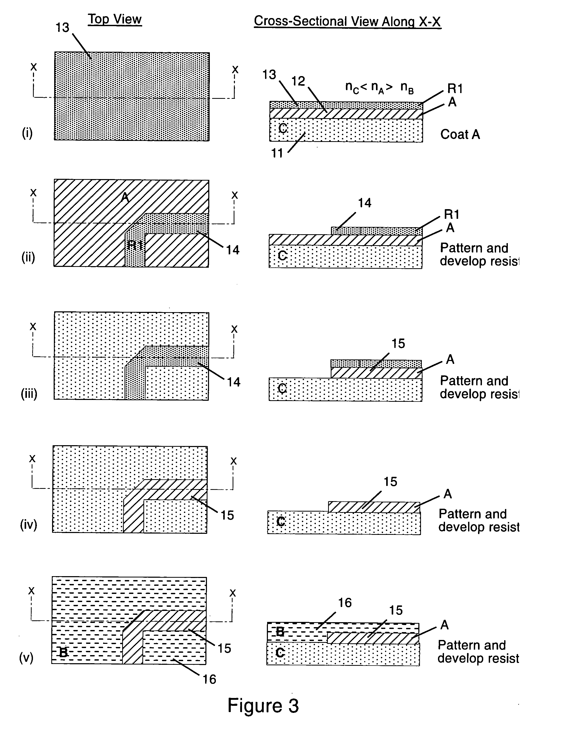
[0085] This process produces 45° facets in channel waveguides. FIG. 3 shows the sequence of steps for this process. On a suitable substrate or underlayer 11 made of material C (such as polycarbonate, polyimide or an acrylic), first the waveguiding (waveguide) layer 12 made of material A is applied by one of various means, such as spinning, dip-coating or laminating. Material A may be another polymer, such as cycloolefincopolymer, or a glass-polymer composite, such as ormosil. A thick photoresist layer 13 of material R1 is applied on top of the waveguide layer. The resist is patterned using a large-area projection lithography system such as has been described in various publications by scientists at Anvik Corporation. The pattern 14 includes the waveguide channels and a 45° facet for a 90° bend. After exposure, the non-waveguide regions of the photoresist are developed away and an etching step then transfers this pattern int...

process embodiment 2

Fabrication of Channel Waveguide with Metallized In-Plane Mirrors

[0088]FIG. 4 illustrates a process which produces metallized 450 mirrors in channel waveguides. First a suitable underlayer 11 of material C is applied followed by a layer 12 of the waveguiding material A, as in Process 1. A photoresist layer 23 of material R1 is then applied in which a rectangular well 24 is patterned and developed away. An etching step then transfers this well into the layer 12 to form deeper well 25. As in Process Embodiment 1, suitable etching techniques include reactive ion etching (RIE) and high-density plasma etching. The etch is stopped at the interface with layer 11 using standard etch stop methods as described above. This is followed by metal (e.g., Al) deposition 26 on the walls of the well, after which the resist 23 is stripped. This removes all of the metal that was deposited on top of the photoresist layer as well as the metal that was deposited along the sides of the well that was in co...

process embodiment 3

Fabrication of Channel Waveguides with Metallized in-Plane Mirrors by Photobleaching

[0091] This process produces channel waveguides by inducing a refractive index differential between the waveguide and the non-guiding regions through photobleaching. As shown in FIG. 5, the steps up to the formation of the well with metallized walls are the same as in Process Embodiment 2. Then, a new resist layer 35 of material R3 is next applied and patterned so that all non-waveguiding regions are opened and the desired metallized wall region is protected. The resist material R3 is chosen so that it both an effective barrier to the subsequent etch step and so that it is opaque to the photobleaching radiation. The sample is now subjected to a directional etching process that removes the unwanted metal, leaving the desired metal facet 30. Next, the sample is uniformly irradiated with appropriate exposure of the photobleaching radiation so that the index of the exposed regions 37 made of modified ma...


PUM


Abstract

Significant advances in semiconductor microelectronics technologies have resulted in greatly enhanced chip performance. Systems studies have continuously shown that on-board interconnects between chips are the bottleneck in achieving board level performance that is comparable with this chip performance. This invention provides a multiple-layer photonic-electronic circuit board family that solves this interconnect performance problem. Multiple layers of patterned optical channel waveguides and patterned electrical conductors co-exist in a single circuit board structure, with optical vias to transport light between different photonics layers and electrical vias to transport electrical signals and power between different electronics layers. An all-lithographic fabrication technology is used to build the entire board structure with mutually compatible planar processing steps. Novel techniques are used to produce channel optical waveguides connected to in-plane 45 degree turning mirrors and channel optical waveguides connected to optical vias with out-of-plane 45 degree turning mirrors. The mirrors can have either total internal reflection or metallized facets.

Description

BACKGROUND OF THE INVENTION [0001] 1. Field of the Invention [0002] This invention relates to a solid-state multiple-layer photonic-electronic circuit board package family, having interconnected layers of photonic circuitry and electronic circuitry. [0003] 2. Description of Related Art [0004] Significant advances in the last two decades in semiconductor microelectronics technologies have resulted in memory chip capacities exceeding one Gigabyte and logic chip speeds exceeding one GigaHertz. Systems studies have continuously shown that on-board interconnects between chips are the bottleneck in achieving a board-level performance that is comparable to the intra-chip data rates. As minimum feature sizes fall below 100 nm, the clock rates of leading-edge microprocessors are expected to exceed 10 GHz in the next few years, further emphasizing the need for faster chip-to-chip interconnects. It is well recognized that a doubling of transistor density in a chip increases the on-board interc...

Claims


Application Information

Patent Timeline
Patent Type & Authority Applications(United States)
IPC IPC(8): G02B6/12G02B6/42G02B6/43H05K1/02
CPCG02B6/4214H05K1/0274G02B2006/12104G02B6/43
Inventor JAIN, KANTIKLING, CARL C.
Owner ANVIK CORP
Why Eureka
Try Eureka