Optical modulator and method of manufacturing same

Inactive Publication Date: 2005-10-06
NEC CORP
View PDF1 Cites 21 Cited by
  • Summary
  • Abstract
  • Description
  • Claims
  • Application Information

AI Technical Summary

Benefits of technology

[0023] The present invention has been made in view of the problems experienced by the conventional optical modulators, and it is an object of the invention to provide a highly sensitive and compact optical modulator which facilitates impedance matching

Problems solved by technology

However, according to the estimates of scholars, the communication infrastructure in Japan will experience shortages of capacity due to rapid increases in the amount of data communications and will become incapable of responding to the demand within five years, at the earliest.
Modulation frequencies beyond 10 GHz cause many optical components to have poor performance.
LD-based direct modulation produces a delay in the change in the density of an injected carrier over time, thus encountering difficulties in modulation at a relaxation oscillation frequency or higher.
An external optical modulator that uses a ferroelectric crystal experiences difficulties in matching the output impedance of a driving source due to a lower impedance of the device, thereby resulting in a failure in providing sufficient modulation characteristics.
Likewise, in electronic circuits and LSIs for processing digital signals, the transmission of signals at higher speeds results in difficulties in the transmission of signals through metal wires particularly between circuits and between chips, so that there is an immediate need for the development of new technologies for optical fiber lines, optical interconnections, and the like.
An expensive optical modulator for optical communications, in which an intensive optical modulator and an edge emission distributed feedback laser are monolithically integrated, is provided.
This device encounters difficulties in forming a thick ferroelectric film to increase voltage sensitivity.
However, any of the prior art optical modulators described above cannot successfully meet all requirements for application in optical communication and optical wiring technologies at 40 Gbps or higher such as faster operation, reduction in driving voltage, reduction in size, an arrayed arrangement, lower cost, and the like.
Further, the Mach-Zehnder optical modulator has limitations when operating at 20 GHz because of difficulties in matching a characteristic impedance of a travelling wave electrode, which is applied with a modulation signal, with a driving source.
The lumped circuit type optical modulator that takes

Method used


Image

  • Optical modulator and method of manufacturing same
  • Optical modulator and method of manufacturing same
  • Optical modulator and method of manufacturing same

Examples


first embodiment

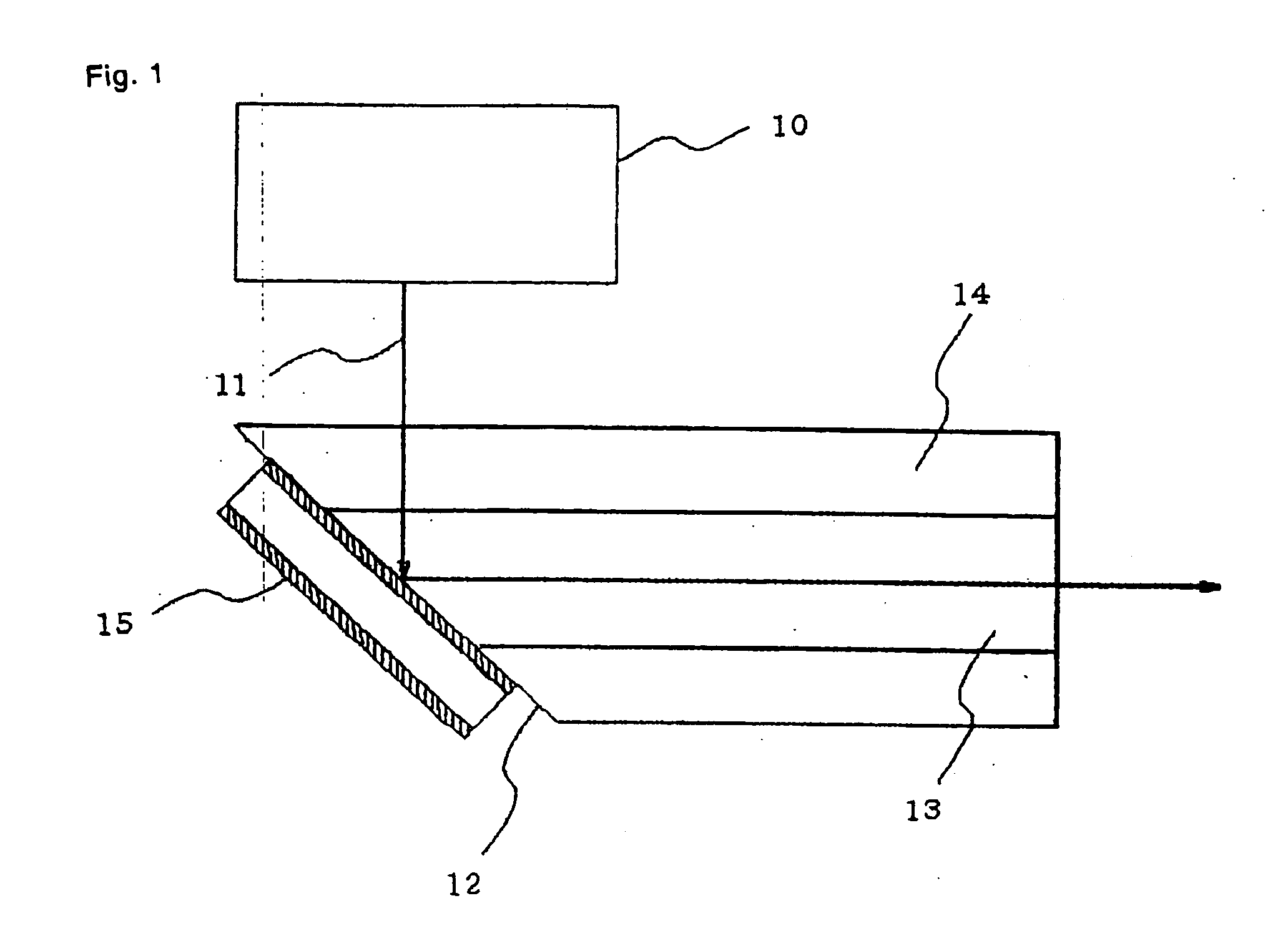
[0060]FIG. 1 illustrates the configuration of a first embodiment of a optical modulation system which includes an optical modulator according to the present invention. Laser light 11 emitted from vertically confined surface emitting laser (VCSEL) 10 is incident on a side surface near an end of optical waveguide 12. Optical waveguide 12 comprises core layer 13, and cladding layer 14 surrounding core layer 13. An end region of optical waveguide 12 is processed by polishing to taper at an angle of 45°, and optical modulator 15 is formed on the polished surface. Optical modulator 15 is placed at such a position that light reflected thereby enters core layer 14 of optical waveguide 12.

[0061] Optical modulator 15 comprises a Fabry-Perot resonator. Light incident on optical modulator 15 repeatedly reflects within and interferes with optical modulator 15, causing a change in the intensity ratio of straight ahead transmitted light to 90° reflected light in accordance with an optical path le...

second embodiment

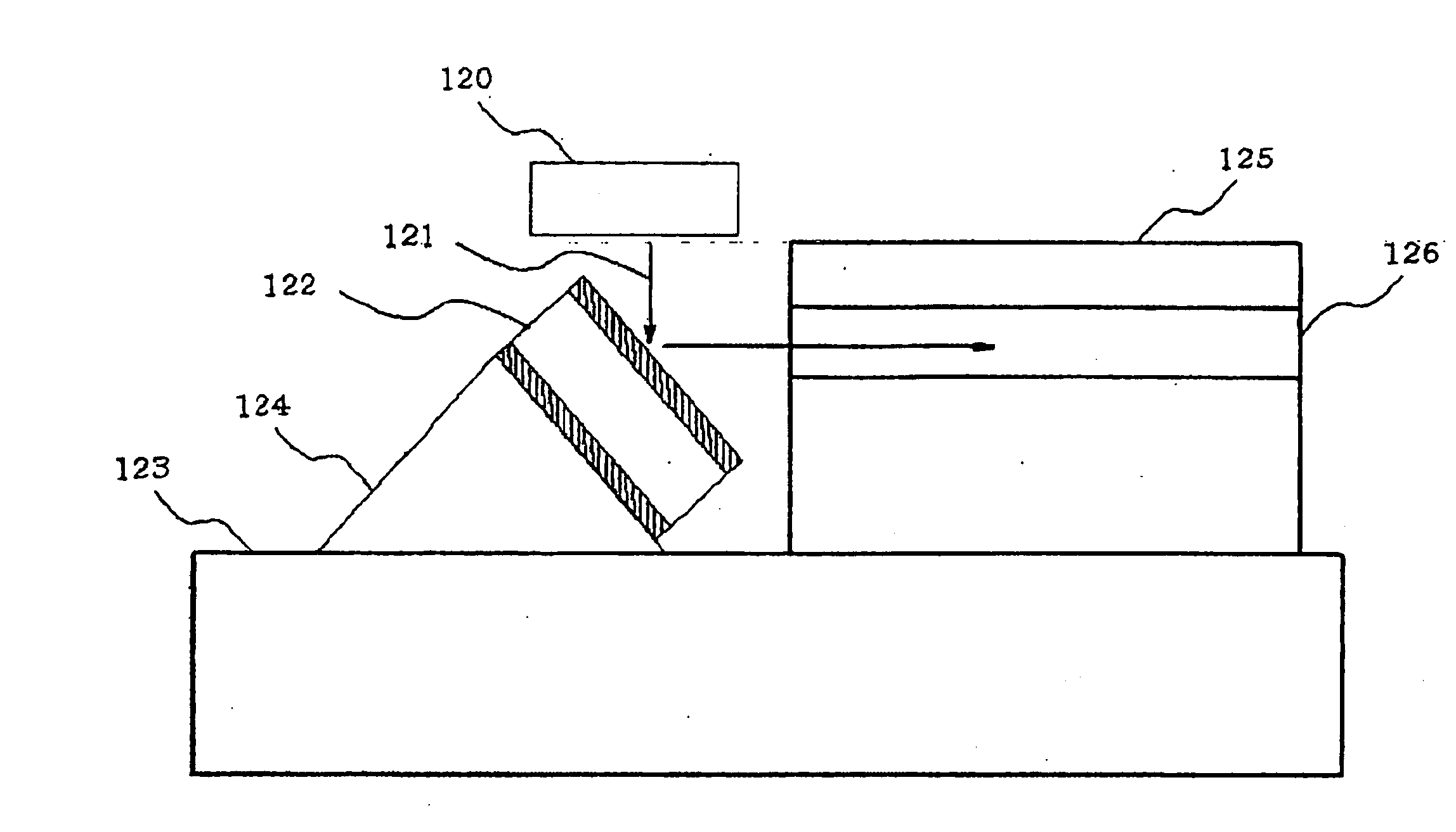
[0096]FIG. 12 illustrates the configuration of a second embodiment of a optical modulation system according to the present invention. Laser light 121 emitted from vertically confined surface emitting laser (VCSEL) 120 is incident on optical modulator 112. Optical modulator 122 is similar in configuration and action to the first to fourth examples of the optical modules described in the first embodiment.

[0097] Optical modulator 122 is formed on the side surface of pyramidal protrusion 124 created on substrate 123. While substrate 123 is made of Si, substrate 123 may be formed of quartz or the like. The shape of pyramidal protrusion 124 can be formed by anisotropic etching of Si. Alternatively, a metal member in a pyramidal shape fabricated by compression molding may adhere to substrate 123 to form protrusive shape 124. Further alternatively, protrusive shape 124 may be formed on substrate 123 by direct molding of low melting point glass. VCSEL 120, optical modulator 122, and optical...

third embodiment

[0098]FIG. 13 illustrates the configuration of a third embodiment of the optical modulation system according to the present invention.

[0099] Laser light 131 emitted from vertically confined surface emitting laser (VCSEL) 130 is incident on optical modulator 132. Optical modulator 132 is formed on the side surface of pyramidal protrusion 134 disposed on substrate 133.

[0100] The side surface of protrusion 134, on which optical modulator 132 is disposed, is shaped into a two-dimensional concave. Optical modulator 132 is in an arcuate shape, as viewed in cross-section, so that the convex of optical modulator 132 fits the shape of the concave of protrusion 134. Light which has undergone optical modulation and travels towards optical waveguide 135 is focused by the concave shape of optical modulator 132. The curvature of the concave shape of optical modulator 132 is set so that the light image emitted by VCSEL 130 is focused on the end surface of optical waveguide 135 and the focused si...


PUM


Abstract

Laser light emitted from a vertically confined surface emitting laser (VCSEL) is incident on a side surface near an end region of an optical waveguide. The end region of the optical waveguide is processed by polishing to taper at an angle of 45 degrees, and an optical modulator is formed on the polished surface. The optical modulator is a Fabry-Perot modulator using a linear electro-optical effect. The modulator has a thick transparent electro-optical layer which is deposited by using an aerosol deposition method.

Description

BACKGROUND OF THE INVENTION [0001] (1) Field of the Invention [0002] The present invention relates to an optical modulator which modulates light from a semiconductor laser or light source at high speeds for transmission, and more particularly, to such an optical module for use in high-speed, large-capacity optical communications and optical interconnections. [0003] (2) Description of the Related Art [0004] Optical communication networks have enabled communication of large quantities of information. However, according to the estimates of scholars, the communication infrastructure in Japan will experience shortages of capacity due to rapid increases in the amount of data communications and will become incapable of responding to the demand within five years, at the earliest. It is said that the tendency for capacity shortage will be accelerated by the proliferation of broadband communications and mobile telephone communications including high quality moving images. [0005] At present, E...

Claims


Application Information

Patent Timeline
IPC IPC(8): G02B6/42G02F1/055G02B6/43G02F1/01G02F1/03G02F1/19H01S5/00H01S5/02H01S5/183
CPCG02B6/42G02B6/4214G02B6/43G02F1/03G02F1/195H01S5/183H01S5/0071H01S5/0085H01S5/02248H01S5/02284H01S5/026G02F2203/023H01S5/02325H01S5/02251
Inventor NAKADA, MASAFUMIOHASHI, KEISHI
Owner NEC CORP
Why Eureka
Try Eureka