Mid-IR microchip laser: ZnS:Cr2+ laser with saturable absorber material

a microchip and absorber material technology, applied in the field ofquantum electronics, can solve the problems of limiting the use of robust low-cost mid-, affecting the quantum efficiency of fluorescence at room temperature, and the source's output power is limited, so as to achieve low-cost mass production and good reproducibility and reliability. the effect of good

Inactive Publication Date: 2005-12-22
UAB RES FOUND
View PDF12 Cites 8 Cited by
  • Summary
  • Abstract
  • Description
  • Claims
  • Application Information

AI Technical Summary

Benefits of technology

[0015] The present invention contemplates a new class of middle-infrared microchip lasers based on transitional metal (TM2+=Ti, V, Cr, Mn, Fe, Co, Ni, and Cu) doped binary II-VI crystals having formula MeZ, where Me being Zn, Cd, Ca, Mg, Sr, Ba, Hg, Pb and Z being S, Se, Te, O and their mixtures as well as mixed ternary chalcogenide matrixes having formula MeX2Z4 with X being Ga, In, Al. A particular embodiment of this invention is microchip laser based on Cr2+ doped ZnS, ZnSe, CdS, and CdSe crystals. The microchip laser is the most compact and simplest diode or fiber laser pumped solid state laser with a typical dimension of 0.5-1 mm3. The main advantages of the proposed microchip lasers will be the ability to be fabricated with collective fabrication processes allowing low cost mass production with good reproducibility and reliability as well as simplicity, allowing its utilization without any optical alignment and maintenance.
[0018] Thermal annealing of the crystals under simultaneous action of electric field for effective thermal diffusion of the dopant into the crystal volume with a temperature and exposition time providing highest concentration of the dopant in the volume without degrading laser performance due to scattering and concentration quenching,
[0023] The present invention further contemplates microchip lasers integrated into “spatially dispersive” cavities for realization of flexible laser modules easily reprogrammable from monochromatic to ultrabroadband and multiline regimes of operation.

Problems solved by technology

Mid-IR wavelengths have also been generated using nonlinearities in Optical Parametric Oscillators3 and difference frequency generators.4,5 All of these approaches yield tunable sources in the mid-IR and all suffer some fundamental problems that limit their use as robust low cost mid-IR source.
Furthermore, to date, all of these sources have limited output powers that preclude their use in higher power applications such as remote sensing.
Long wavelength TM emissions are quenched by multi-photon processes in conventional laser host media such as oxide and fluoride crystals, resulting in extremely low room-temperature quantum efficiency of fluorescence.
Finally, a key feature of these materials is a poor phonon spectrum that makes them transparent in a wide spectral region, decreases the efficiency of non-radiative decay and gives promise to a high yield of fluorescence at room temperature.
However, in these spectroscopic and laser studies of TM2+:II-VI materials there was no indication that microchip lasers and chip-scaled integrated lasers could be designed on the basis of TM doped II-VI hosts.
Finally, the prior art has not taught utilization of acousto-optic, electro-optic, photorefractive and birefringent properties of II-VI crystals in one integrated microchip system combining active medium, acousto- or electro-optic modulator, filter, other passive components of the cavity such as waveguide grating, or birefringent filter.

Method used


Image

  • Mid-IR microchip laser: ZnS:Cr2+ laser with saturable absorber material
  • Mid-IR microchip laser: ZnS:Cr2+ laser with saturable absorber material
  • Mid-IR microchip laser: ZnS:Cr2+ laser with saturable absorber material

Examples


Embodiment Construction

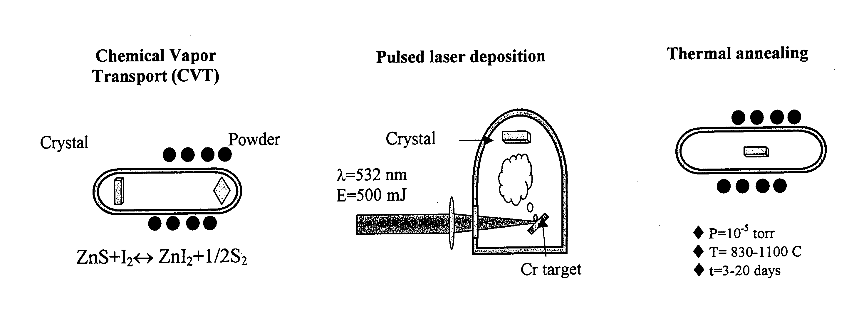
[0045] In the preferred embodiment, the Cr2+:ZnS crystals are prepared by a three-stage method according to a flow chart depicted in FIG. 1. At the first stage, undoped single crystals are synthesized by a chemical transport reaction from gas phase using an iodine gas transport scheme, preferably in a quartz tube 20mm in diameter and 200mm in length placed in a two heating zone furnace. Powder obtained by a joint ignition of initial components serves as raw material. Temperatures in the zones of raw material and crystallization are approximately 1200° C. and 1100° C. respectively. I2 concentration is in the range of 2-5 mg / cm3. High optical quality unoriented ingots, preferably Ø2×cm3, are cut and ground to slabs of 5×5×3 mm size.

[0046] At the second stage and third stages, introduction of chromium (or other transitional metal) into the crystalline host is performed by thermal diffusion (third stage) from a then film deposited, preferably, by the pulse laser deposition method (seco...


PUM

PropertyMeasurementUnit
thicknessaaaaaaaaaa
concentrationaaaaaaaaaa
sizeaaaaaaaaaa

Abstract

A method of fabrication of laser gain material and utilization of such media includes the steps of introducing a transitional metal, preferably Cr2+ thin film of controllable thickness on the ZnS crystal facets after crystal growth by means of pulse laser deposition or plasma sputtering, thermal annealing of the crystals for effective thermal diffusion of the dopant into the crystal volume with a temperature and exposition time providing the highest concentration of the dopant in the volume without degrading laser performance due to scattering and concentration quenching, and formation of a microchip laser either by means of direct deposition of mirrors on flat and parallel polished facets of a thin Cr:ZnS wafer or by relying on the internal reflectance of such facets. The gain material is susceptible to utilization of direct diode or fiber laser pumping of a microchip laser with a level of power density providing formation of positive lens and corresponding cavity stabilization as well as threshold population inversion in the laser material. Multiple applications of the laser material are contemplated in the invention.

Description

[0001] This patent application is a divisional of U.S. patent application Ser. No. 10 / 247,272 which was filed on Sep. 19, 2002FIELD OF THE INVENTION [0002] The present invention relates to the field of Quantum Electronics, and more particularly to the elemental basis of laser technology, and can be used to develop tunable mid-infrared (mid-IR) solid state lasers. [0003] Primarily, the invention can be used in cases where monochromatic laser emissions tunable in the middle-infrared spectral region are required for solving problems in various fields of science and technology, such as laser spectroscopy, trace gas analysis, photo chemistry, photo biology, medicine, and wavelength specific military applications, among others. BACKGROUND OF THE INVENTION [0004] There is a growing demand for affordable mid-infrared sources for use in a variety of applications including atmospheric sensing (global wind sensing and low altitude wind shear detection), eye-safe medical laser sources for non-i...

Claims


Application Information

Patent Timeline
Patent Type & Authority Applications(United States)
IPC IPC(8): H01S3/16C30B31/00C30B31/02H01S3/06H01S3/08H01S3/081H01S3/094H01S3/0941H01S3/1055H01S3/113
CPCC30B31/00H01S3/117H01S3/0014H01S3/0604H01S3/0627H01S3/08009H01S3/08086H01S3/094038H01S3/094042H01S3/09415H01S3/1055H01S3/113H01S3/162H01S3/1623H01S3/1628H01S2301/04C30B31/02H01S3/115Y10S438/917H01S3/108H01S3/094046H01S3/0805C30B29/48H01S3/0617
Inventor MIRROR, SERGEY B.FEDEROV, VLADIMIR V.
Owner UAB RES FOUND
Why Eureka
Try Eureka