Formation of nanowhiskers on a substrate of dissimilar material

a technology of dissimilar materials and nanowhiskers, applied in the direction of polycrystalline material growth, crystal growth process, chemically reactive gas, etc., can solve the problems of large thermal expansion coefficient difference, defective material, and formation of anti-phase domain walls, so as to achieve high-reliability photonics devices, effective implementation of optical interconnections, and the effect of essentially constant luminescence properties of segments

Inactive Publication Date: 2006-06-15
QUNANO
View PDF45 Cites 90 Cited by
  • Summary
  • Abstract
  • Description
  • Claims
  • Application Information

AI Technical Summary

Benefits of technology

[0062] Further, the luminescence properties of the segment remain essentially constant, with substantially no quenching, from cryogenic temperatures up to room temperature, thereby providing for highly reliable photonics devices. In accordance with the invention, the provision of nanowhiskers containing optically active material on a silicon substrate permits a very effective implementation of optical i

Problems solved by technology

Epitaxial growth of III-V semiconductors on Si presents a number of difficulties, such as lattice mismatch, differences in crystal structure (III-V's have a polar zinc blende or wurtzite structure whereas Si has a covalent diamond structure), and a large difference in thermal

Method used


Image

  • Formation of nanowhiskers on a substrate of dissimilar material
  • Formation of nanowhiskers on a substrate of dissimilar material
  • Formation of nanowhiskers on a substrate of dissimilar material

Examples


examples

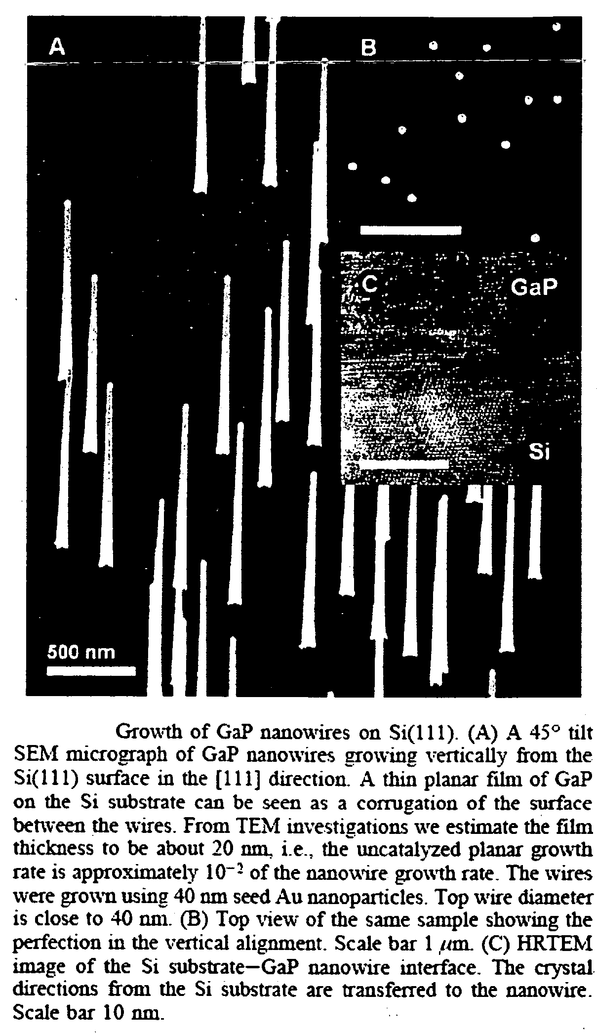
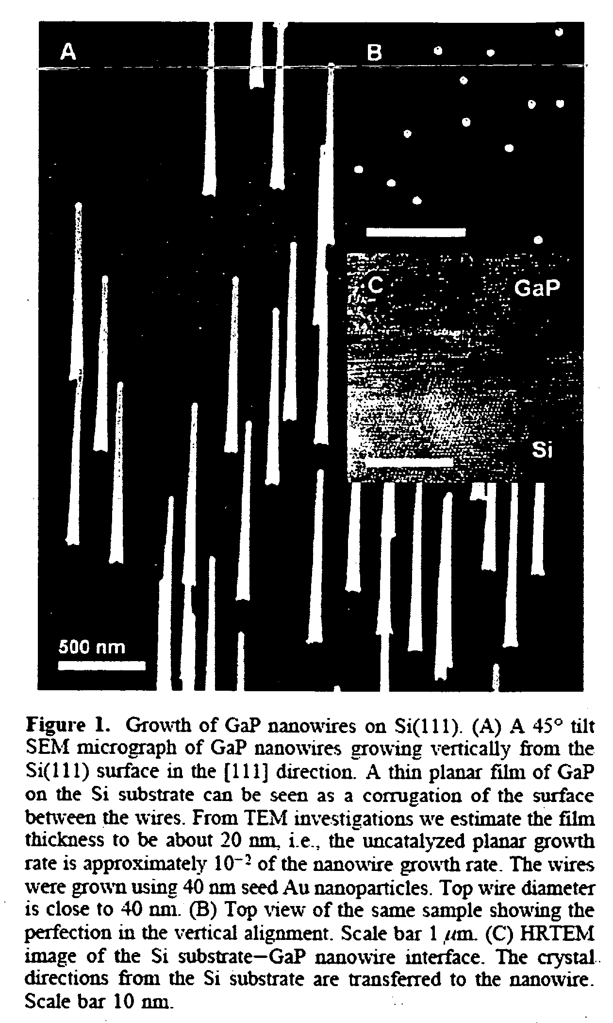
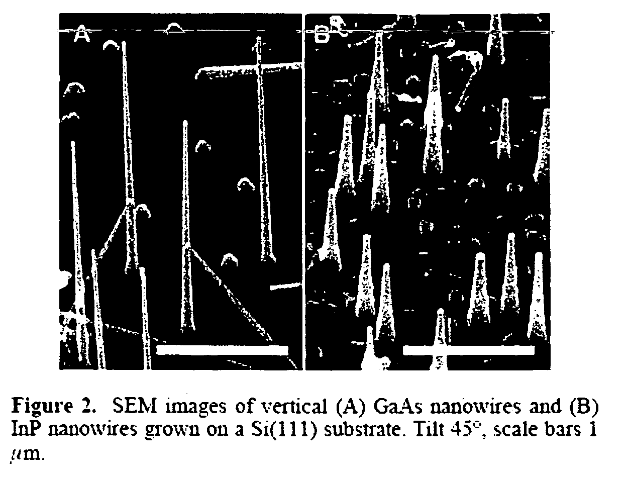
[0076] Starting material was “Toyo” Epitaxial Silicon Wafers, P type substrate with a P type epilayer orientation (111).

DopantResistivityThicknessSubstrateBoronΩ cm245 μmLayerBoron12Ω cm 27 μm

[0077] Preparation Prior to Growth

[0078] 1) Clean with ultrasonic Tri-clean to remove organic residues and particles.

[0079] The wafer was placed in a test tube and solution a) below was added. The test tube was put in ultrasonic bath at 35 KHz for 2-3 minutes. After, the bath the solution was decanted and the next solution was added. The process repeated for solutions b)-d) in that order.

[0080] a) Trichloroethylene (proanalysi)

[0081] b) Acetone (proanalysi)

[0082] c) Ethanol (95%)

[0083] d) Milli-Q-H2O

[0084] The water was decanted and refilled 2-3 times in Milli-Q-H2O (18.2 W cm 25° C.). Rinse the wafer.)

[0085] 2) The wafer was removed from the rinse water and immediately cleaned with Piranha Etch to remove any remaining organic residues.

[0086] The following were measured and mixed in ...


PUM


Abstract

A method for forming a nanowhisker of, e.g., a III-V semiconductor material on a silicon substrate, comprises: preparing a surface of the silicon substrate with measures including passivating the substrate surface by HF etching, so that the substrate surface is essentially atomically flat. Catalytic particles on the substrate surface are deposited from an aerosol; the substrate is annealed; and gases for a MOVPE process are introduced into the atmosphere surrounding the substrate, so that nanowhiskers are grown by the VLS mechanism. In the grown nanowhisker, the crystal directions of the substrate are transferred to the epitaxial crystal planes at the base of the nanowhisker and adjacent the substrate surface. A segment of an optically active material may be formed within the nanowhisker and bounded by heterojunctions so as to create a quantum well wherein the height of the quantum well is much greater than the thermal energy at room temperature, whereby the luminescence properties of the segment remain constant without quenching from cryogenic temperatures up to room temperature.

Description

CROSS-REFERENCE TO RELATED APPLICATIONS [0001] This application claims the benefit of the priority of U.S. Provisional Patent Application No. 60 / 582,513, filed Jun. 25, 2004, the entirety of which is incorporated herein by reference.BACKGROUND OF THE INVENTION [0002] 1. Field of the Invention [0003] This invention relates generally to structures produced by techniques of nanotechnology, and methods of producing such structures. [0004] More specifically, the invention relates to such structures and devices incorporating at least one element, essentially in one-dimensional form, which is of nanometer dimensions in its width or diameter, which is produced with the aid of a catalytic particle, and which is commonly termed a “nanowhisker.”[0005] The invention relates also to a method of forming a nanowhisker of a certain material on a substrate of a dissimilar material. [0006] 2. Brief Description of the Prior Art [0007] Nanotechnology covers various fields, including that of nanoenginee...

Claims


Application Information

Patent Timeline
IPC IPC(8): H01L29/12
CPCB82Y30/00C30B11/12C30B25/005C30B29/40C30B29/48C30B29/60C30B29/605H01L21/02381H01L21/02543H01L21/02546H01L21/02551H01L21/02603H01L21/0262H01L21/02639H01L21/02645H01L33/0066Y10S977/89Y10S977/762Y10S977/891Y10S977/815
Inventor SAMUELSON, LARS IVARMARTENSSON, THOMAS M.I.
Owner QUNANO
Why Eureka
Try Eureka