
Field effect transistor, method of producing the same, and method of producing laminated member

a field effect transistor and field effect technology, applied in the direction of thermoelectric device junction materials, electrical apparatus, semiconductor devices, etc., can solve the problems of deterioration, never be said, excellent mobilities described in those publications

Inactive Publication Date: 2007-01-18
CANON KK
View PDF9 Cites 43 Cited by
  • Summary
  • Abstract
  • Description
  • Claims
  • Application Information

AI Technical Summary

Benefits of technology

[0008] The present invention has been made in order to solve the above problems, and an object of the present invention is to provide a field effect transistor which enables an organic semiconductor layer having high crystallinity and high orientation to be formed and which exhibits a high field effect mobility.
[0009] Another object of the present invention is to provide a method of producing a field effect transistor which enables the above field effect transistor to be easily obtained.

Problems solved by technology

The pentacene thin film produced by means of vacuum vapor deposition is known to exhibit a high field effect mobility, but involves a problem in that the pentacene thin film is unstable in the air, is susceptible to oxidation, and is thus apt to deteriorate.
However, it can never be said that the carrier mobilities described in those publications are excellent.
However, there has involved a problem in that the acene is susceptible to oxidation, and is thus apt to deteriorate.

Method used


Image

  • Field effect transistor, method of producing the same, and method of producing laminated member
  • Field effect transistor, method of producing the same, and method of producing laminated member
  • Field effect transistor, method of producing the same, and method of producing laminated member

Examples


synthesis example 1

(Step 1-1)

[0123] A mixed solution of 3.16 g (39.5 mmol) of 1,3-cyclohexadiene, 10.5 g (34.1 mmol) of trans-1,2-bis(phenylsulfonyl)ethylene, and 200 ml of toluene was refluxed for 7 hours. After that, the solution was cooled and concentrated under reduced pressure to yield a reaction mixture. The reaction crude product was recrystallized (chloroform / hexane) to yield 5,6-bis(phenylsulfonyl)-bicyclo[2.2.2]octa-2-ene (13.8 g, 35.6 mmol, 90% yield).

(Step 1-2)

[0124] The reaction system of a mixed solution of 7.76 g (20 mmol) of the resultant 5,6-bis(phenylsulfonyl)-bicyclo[2.2.2]octa-2-ene and 50 ml of anhydrous tetrahydrofuran was replaced with nitrogen. Then, 2.425 ml (22 mmol) of ethyl isocyanoacetate were added to the solution, and the mixture was cooled to 0° C. Potassium t-butoxide (50 ml / l M THF (tetrahydrofuran) solution) was dropped over 2 hours, and the whole was stirred at room temperature for 3 hours. After the completion of the reaction, dilute hydrochloric acid was adde...

synthesis example 2

(Step 2-1)

[0127] 2,4-pentanedione (205.4 ml, 2.0 mol), acetone (100 ml), n-butyl bromide (54 ml, 0.5 mol), and potassium carbonate (34.55 g, 0.25 mol) were fed into a reaction vessel, and the mixture was replaced with nitrogen, followed by reflux for 48 hours. The resultant solid was filtered out, and the solvent was distilled off by means of an evaporator. After that, unreacted 2,4-pentanedione was distilled off under reduced pressure by means of a diaphragm. Then, the remainder was distilled in a vacuum to yield 3-n-butyl 2,4-petanedione (43.25 g, 55% yield).

(Step 2-2)

[0128] Benzyl acetoacetate (97 ml, 560 mmol) and acetic acid (81 ml) were fed into a reaction vessel. Then, a solution of sodium nitrite (37.8 g) in water (115 ml) was dropped into the mixture at 10° C. or lower. After the dropping, the mixture was stirred for 3 hours at room temperature. A solution of 3-n-butyl 2,4-pentanedione (43.16 g, 280 mmol) obtained in Step 2-1 in acetic acid (45 ml), a mixture of zinc p...

example 1

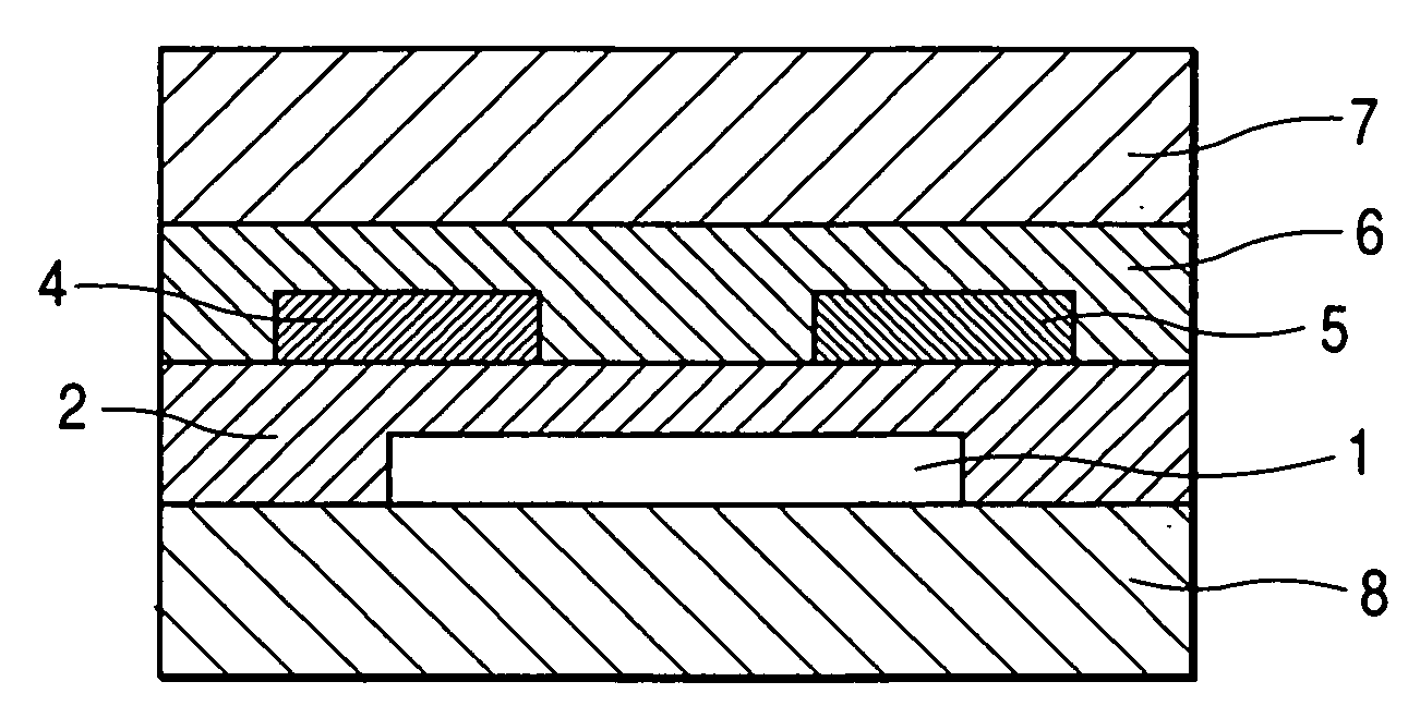
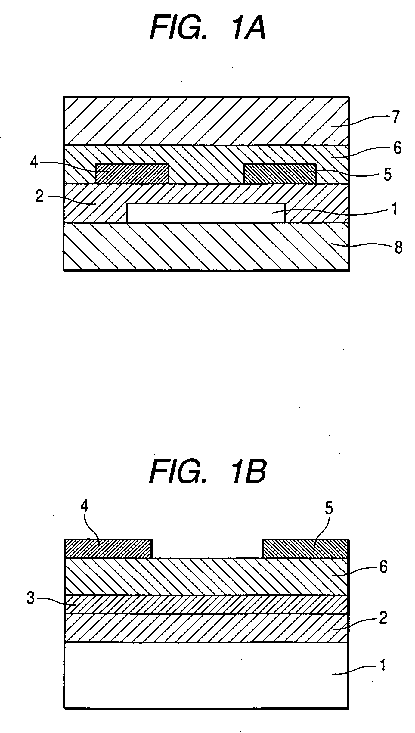
[0144]FIG. 1B shows the structure of a field effect transistor in this example.

[0145] First, a highly doped N type silicon substrate was provided as the gate electrode 1. A silicon oxide film having a thickness of 5,000 Å obtained by thermal oxidation of the surface layer of the silicon substrate was provided as the insulating layer 2. Next, the resin solution a was applied to the surface of the insulating layer by means of a spin coating method (at a number of revolutions of 5,000 rpm). Next, the applied film was moved onto a hot plate and heated at 100° C. for 5 minutes and 200° C. for 20 minutes. Measurement with stylus-type step difference measuring device showed that the film had a thickness of 50 nm. The film was provided as the A layer 3 (polysiloxane layer).

[0146] Next, the metal-free tetrabicyclo compound synthesized in Synthesis Example (1) in powder form was heated in a vacuum at 200° C. to be transformed into a benzo compound, and was then formed into a film on the sub...


PUM


Abstract

There is provided a field effect transistor having an organic semiconductor layer, including: an organic semiconductor layer containing at least porphyrin; and a layer composed of at least a polysiloxane compound, the layer being laminated on the organic semiconductor layer so as to be in intimate contact with the organic semiconductor layer. As a result, there can be provided a field effect transistor which enables an organic semiconductor layer having high crystallinity and high orientation to be formed and which exhibits a high mobility.

Description

TECHNICAL FIELD [0001] The present invention relates to a field effect transistor, a method of producing the field effect transistor, and a method of producing a laminated member. BACKGROUND ART [0002] Development of a thin film transistor using an organic semiconductor has gradually become active since the latter half of 1980s. In recent years, the basic performance of the thin film transistor using the organic semiconductor has exceeded the properties of a thin film transistor of amorphous silicon. The use of an organic material as a semiconductor layer in a thin film device is attractive because the organic material can be easily processed and often has a high affinity for a plastic substrate on which a thin film field effect transistor (FET) is formed. Examples of the researches on organic semiconductors reported heretofore include: acenes such as pentacene and tetracene disclosed in Japanese Patent Application Laid-Open No. H05-55568; phthalocyanines including lead phthalocyani...

Claims


Application Information

Patent Timeline
IPC IPC(8): H01L29/08H01L51/00H01L51/05
CPCH01L51/0012H01L51/0077H01L51/0545H01L51/0512H01L51/0533H01L51/0078H10K71/191H10K85/311H10K85/30H10K10/462H10K10/476H10K10/466
Inventor MIURA, DAISUKENAKAYAMA, TOMONARIOHNISHI, TOSHINOBUKUBOTA, MAKOTOMASUMOTO, AKANETSUZUKI, HIDETOSHIMIYACHI, MAKIKO
Owner CANON KK
Learn More