Nanoparticles and Their Use for Multifunctional Bioimaging
- Summary
- Abstract
- Description
- Claims
- Application Information
AI Technical Summary
Benefits of technology
Problems solved by technology
Method used
Image
Examples
example 1
Core / Shell Structure and Size of Nanocrystals
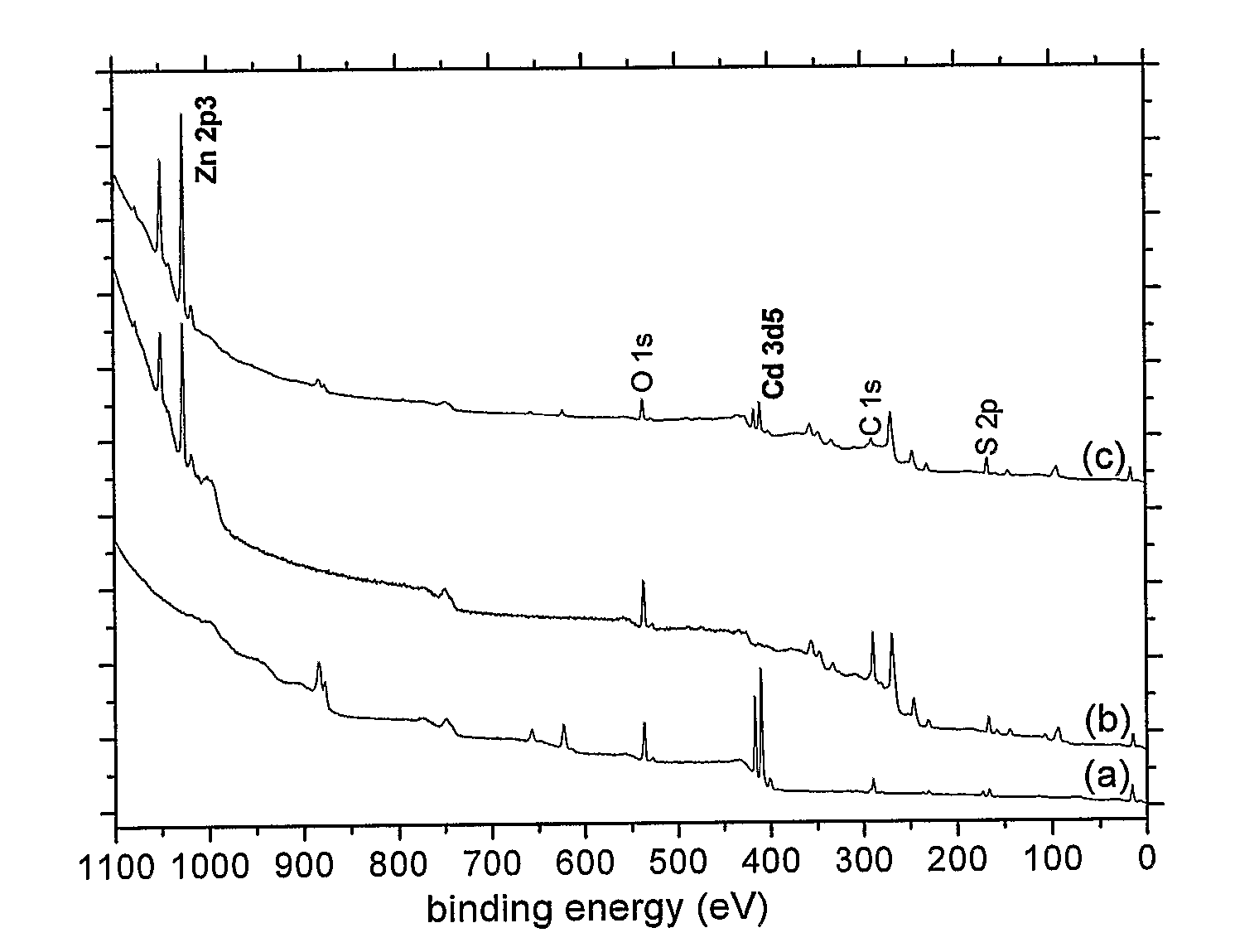
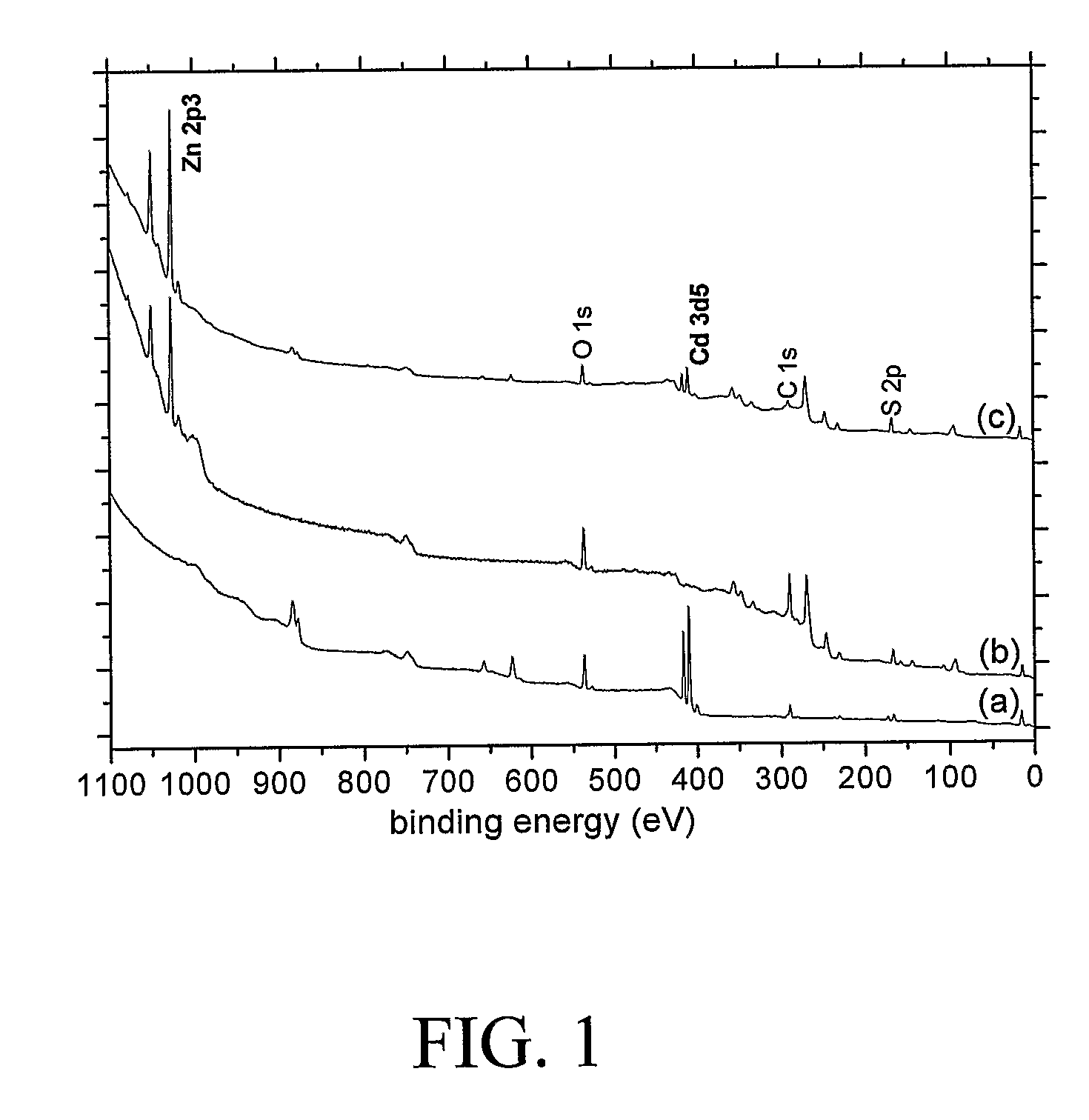
[0166] It has been reported that synthesized nanocrystals consist of a CdS core / ZnS shell structure, based on UV-visible absorption spectroscopy and x-ray photoelectron spectroscopy (XPS) / energy-dispersive spectroscopy (EDS) (Yang, H. and P. H. Holloway, Appl. Phys. Lett. 2003, 82:1965-1967). Since XPS is a surface sensitive method and EDS is a ‘bulk’ method of analysis (Brundle, C. R., Encyclopedia of Materials Characterization, (Eds: C. R. Brundle, C. A. Evans, Jr., S. Wilson), Butterworth-Heinemann, Boston 1992), the samples with CdS core / ZnS shell structure should experience an attenuation of the signals from buried core element, i.e., Cd, in XPS relative to EDS. Thus XPS spectra should be dominated by the shell, while EDS spectra should exhibit the elements in both the shell and the core structure averaged over many nanocrystal thickness. XPS survey spectra of CdS:Mn, ZnS:Mn, and CdS:Mn / ZnS core / shell nanocrystals are shown in FIG. ...
example 2
Photoluminescence (PL) and Quantum Yield
[0167] PL emission spectra, obtained using 325 nm HeCd laser excitation, of n-dodecanethiol-passivated and ZnS-passivated CdS:Mn nanocrystals are compared in FIG. 3A and FIG. 3B, respectively. Note that PL measurements were carried out in the solid-state sample, i.e., ˜200 nm thick CdS:Mn / ZnS nanocrystal layers on the glass substrate. The Mn2+ 4T1-6A1 transition at ˜600 nm is observed from both nanocrystalline samples. In addition to the Mn emission at ˜600 nm, emission from a surface-related defect (shallow trap) is observed at ˜450 nm from organically passivated nanocrystals. This defect emission originates from the localized surface states in the band gap, which presumably are formed by the lack of bonding to surface S ions. In contrast, no defect-related emission is observed from inorganically passivated nanocrystals, indicating the successful complete passivation of CdS:Mn core surface by the ZnS shell layer.
[0168] The quantum yields of...
example 3
Effects of UV irradiation and Photooxidation
[0169] The change of PL emission intensity from organically and inorganically passivated CdS:Mn during 400 nm UV irradiation was monitored at room temperature using a monochromatized 300 W Xe light source (FIG. 5). The 400 nm UV irradiation was estimated to have a powder density of 655 μW / cm2. Organically passivated CdS:Mn nanocrystals exhibit a significant reduction (˜45% after 3 hours) of the PL emission intensity upon UV exposure, while CdS:Mn / ZnS core / shell nanocrystals show an increased PL intensity (˜40% after 3 hours). The reduced PL emission intensity of n-dodecanethiol-passivated CdS:Mn nanocrystals presumably results from the fact that the bonding between the Cd (from nanocrystal) and S ions (from organic passivating species) at the surface is deteriorated by UV exposure. Accordingly, the density of nonradiative relaxation paths increases at the surface, resulting in a decreased PL emission intensity (C. Jin, C., J. Yu, L. Sun, ...
PUM
| Property | Measurement | Unit |
|---|---|---|
| Magnetic field | aaaaa | aaaaa |
| Volume | aaaaa | aaaaa |
| Volume | aaaaa | aaaaa |
Abstract
Description
Claims
Application Information


