Transparent substrate with thin film and method for manufacturing transparent substrate with circuit pattern wherein such transparent substrate with thin film is used
a technology of transparent substrate and thin film, which is applied in the direction of conductive layer on the insulating support, electric discharge tube/lamp manufacturing, and conductive material removal by irradiation. it can solve the problems of over-high production cost, poor yield, and significant increase in production cost. reduce the number of steps, reduce the cost of production and environmental burden, reduce the effect of production cos
- Summary
- Abstract
- Description
- Claims
- Application Information
AI Technical Summary
Benefits of technology
Problems solved by technology
Method used
Image
Examples
examples
[0096]The invention will be illustrated in greater detail by reference to the following Examples, but the invention should not be construed as being limited to the following Examples. Incidentally, Examples 1 to 5 are Invention Examples and Examples 6 to 9 are Comparative Examples.
examples 1 to 4 and examples 6 to 9
[0097]A glass substrate which was 40 mm square and had a thickness of 2.8 mm (PD200, manufactured by Asahi Glass Co., Ltd.) was prepared. A tin oxide thin film was formed on a surface of the substrate by the following method.
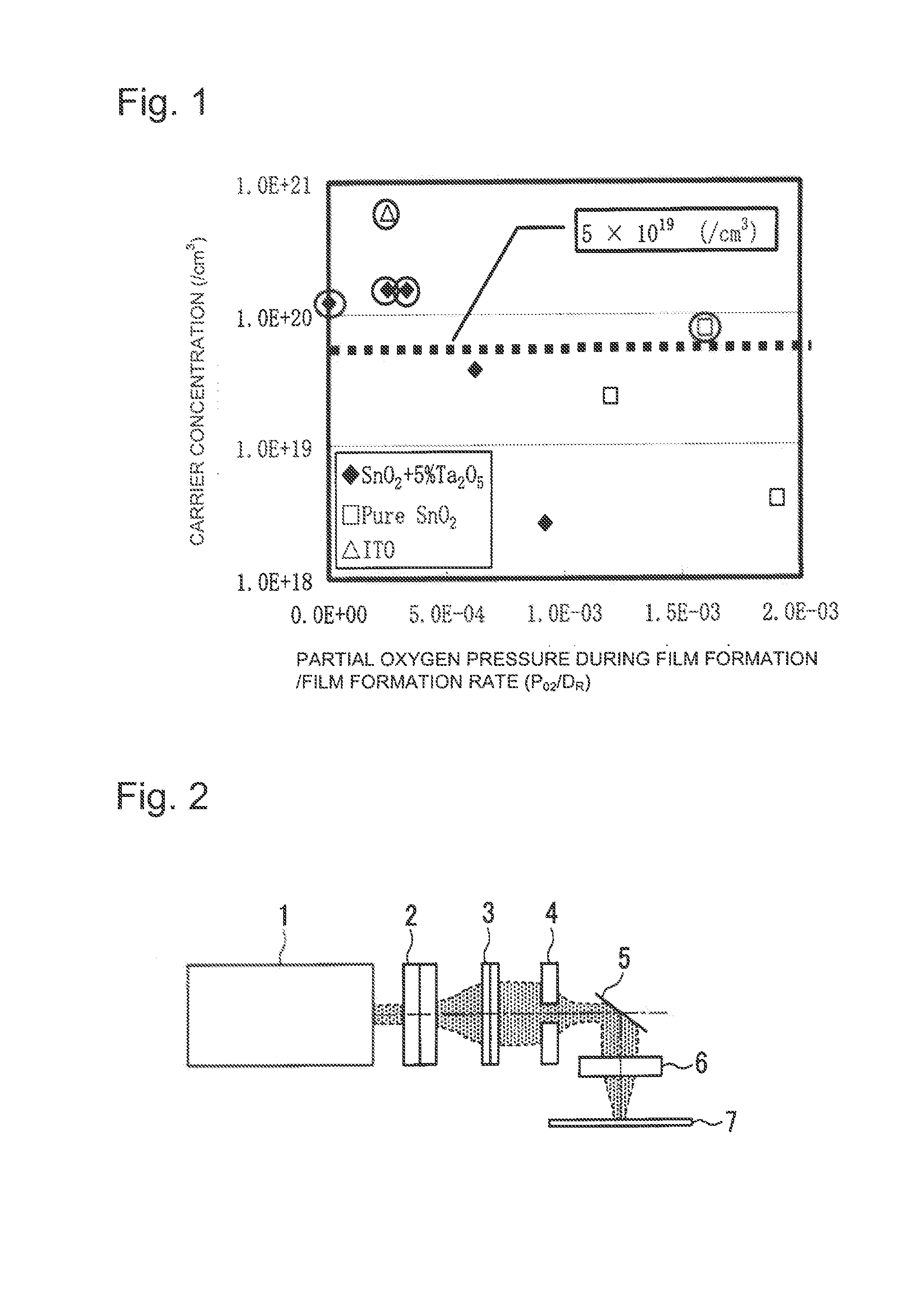
[0098]Film formation of a tin oxide thin film was carried out by ion plating using, as a raw vapor deposition material, an SnO2 sinter containing neither tantalum nor antimony nor fluorine or an SnO2 sinter containing Ta2O5 in an amount of 5% by mass based on the whole, while changing partial oxygen pressure during the film formation and film formation rate. The film formed had the same composition as the sinter.
example 5
[0099]A glass substrate which was 40 mm square and had a thickness of 2.8 mm (PD200, manufactured by Asahi Glass Co., Ltd.) was prepared. An ITO thin film was formed on a surface of the substrate by the following method.
[0100]Film formation was carried out by sputtering using an ITO sinter target composed of indium oxide and SnO2 added thereto in an amount of 10% by mass based on the whole. The film formed had the same composition as the sinter.
[0101]The film thickness (D [nm]), partial oxygen pressure during film formation / film formation rate (Po2 / DR [Pa / (Å / sec)]), carrier concentration (n [1 / cm3]), and laser energy (E [J / cm2]) for each of the samples of Examples 1 to 9 are shown in Table 1. Incidentally, the partial oxygen pressure during film formation / film formation rate (Po2 / DR) means the ratio of partial oxygen pressure during film formation relative to film formation rate.
[0102]The carrier concentration was determined with equation (1) from the value of mobility measured by a...
PUM
| Property | Measurement | Unit |
|---|---|---|
| thickness | aaaaa | aaaaa |
| wavelength | aaaaa | aaaaa |
| transparent conductive | aaaaa | aaaaa |
Abstract
Description
Claims
Application Information


