Metal oxide semiconductor, semiconductor element, thin film transistor and method of manufacturing thereof

a metal oxide semiconductor and manufacturing method technology, applied in the direction of semiconductor devices, basic electric elements, electrical appliances, etc., can solve the problems of difficult application of light and flexible resin substrates, low energy efficiency, and relatively long processing time, and achieve high manufacturing efficiency

Active Publication Date: 2009-07-09
KONICA MINOLTA INC
View PDF1 Cites 69 Cited by
  • Summary
  • Abstract
  • Description
  • Claims
  • Application Information

AI Technical Summary

Benefits of technology

[0015]An object of the present invention is to provide a method of manufacturing a metal oxide semiconductor layer by carrying out a transformation treatment to a semiconductor with a high manufacturing efficiency, in which film formation can be carried out via a coating process (for example, a printing method or an inkjet method) under an atmospheric pressure using a metal salt as a precursor, and, further, a low temperature manufacturing is possible, and to provide a TFT element obtained by using the method.

Problems solved by technology

Accordingly, the energy efficiency is not high, a relatively long processing time is needed, and the application of a light and flexible resin substrate becomes difficult because the temperature of the substrate increases as high as the treatment temperature while being treated.
In the case of plasma oxidation, since the treatment is carried out in an extremely reactive plasma space, there has been a problem that the electrode or the insulating layer is degraded in the thin film transistor manufacturing process, whereby the mobility and the off electric current (dark current) turns worse.
Also, a method to obtain a metal oxide semiconductor via such as a thermal oxidation using an organic metal or a metal salt as a precursor has been known (for example, refer to Non-Patent Document 1, 2, or 3) For example, when a metal alkoxide is used as a precursor, there may be a problem that the property may deteriorate due to remaining carbon, as well as a problem that a high temperature treatment is needed, or, when a chloride is used as a precursor, there may be a problem that halogen is evacuated.
These precursors also have a problem that the precursors may be hydrolyzed by the water contained in the atmosphere, and, further, these precursors need a big amount of organic solvents, which is not preferred in view of the circumstance problem.
Moreover, there have been problems that the thin film transistor (TFT) produced by using these metal oxide semiconductors exhibits a lower mobility, a smaller on / off ratio and a larger threshold value.
There may be a problem in the method using a vacuum apparatus such as sputtering that the manufacturing efficiency is not high, because a batch production is needed in such a method.
Also, there has been a problem that the metal oxide semiconductor manufactured by using a sputtering method tends to have a property variation, and that a high temperature treatment after the production is needed to stabilize the property.

Method used


Image

  • Metal oxide semiconductor, semiconductor element, thin film transistor and method of manufacturing thereof
  • Metal oxide semiconductor, semiconductor element, thin film transistor and method of manufacturing thereof
  • Metal oxide semiconductor, semiconductor element, thin film transistor and method of manufacturing thereof

Examples


example 1

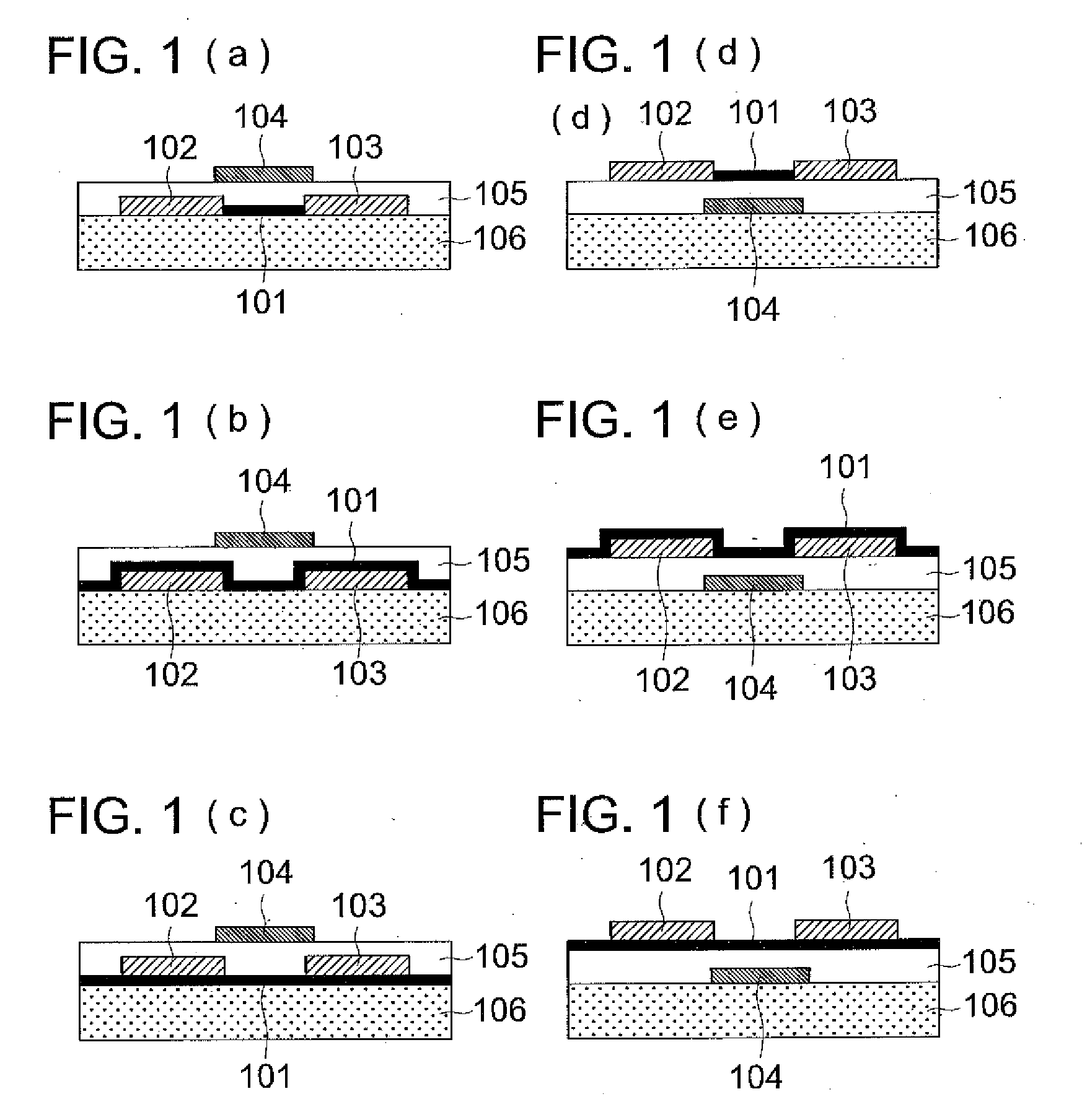
[0122]In FIGS. 3(1)-3(4), schematic cross-sectional views illustrating the manufacturing process of a thin film transistor are shown.

(Manufacturing of Thin Film Transistor Element 1)

[0123]As substrate 6, an alkali-free glass substrate was used, and an ITO film having a thickness of 150 nm was formed all over the substrate by sputtering. Then, the ITO film was subjected to patterning via photolithography to form gate electrode 4.

[0124]Subsequently, gate insulating layer 5 composed of 200 nm thick silicon oxide was formed by an atmospheric pressure plasma CVD method. The atmospheric pressure plasma treatment apparatus disclosed in FIG. 6 of JP-A No. 2003-303520 was used.

(Gases used)Inert gas: helium98.25%by volumeReactive gas: oxygen gas1.5%by volumeReactive gas: tetraethoxysilane vapor0.25%by volume(bubbled with helium gas)

(Discharge conditions)High frequency power source:13.56MHzDischarge power:10W / cm2

(Electrode Conditions)

[0125]The electrode is a grounded roll electrode having a di...

example 2

[0159]Similarly, a bottom gate-top contact thin film transistor element of which schematic cross-sections were shown in FIGS. 4(1)-4(5) were manufactured.

[0160]A polyimide film (200 μm in thickness) was used as substrate 6. Corona discharge treatment was carried out at a condition of 50 W / m2 / min on the substrate, followed by forming a subbing layer as follows to improve the adhesion.

(Formation of Subbing Layer)

[0161]The coating liquid having the following composition was applied so that the dry thickness was 2 μm, followed by drying at 90° C. for 5 minutes, and then was subjected to hardening using a high-pressure mercury lamp of 60 W / cm at a distance of 10 cm for 4 seconds.

Dipentaerythritol hexaacrylate monomer60gDipentaerythritol hexaacrylate dimer20gComponent of dipentaerythritol hexaacrylate trimer or larger20gDiethoxybenzophenone UV initiator2gSilicone surfactant1gMethylethyl ketone75gMethylpropyleneglycol75g

[0162]Further, atmospheric pressure plasma treatment was continuously ...

example 3

[0176]Thin film transistor elements having different compositions were manufactured by varying the ratio of indium nitrate [In(NO3)3], zinc nitrate [Zn(NO3)2] and gallium nitrate [Ga(NO3)3] as raw materials of the semiconductor precursor (FIG. 5).

[0177]On a silicon wafer having a specific resistance of 0.02 Ω / cm as gate electrode 4, a 2000 Å thick of thermal oxidation film was formed to obtain gate insulating layer 5.

[0178]Hereafter, this is called as a substrate. The substrate was then cleaned by being irradiated with a UV light for 10 minutes at 70° C. under a circumstance of ozone.

[0179]Next, a metal salt coating solution was prepared as a precursor material.

[0180]The nitrates of In, Ga, and Zn were mixed and dissolved in pure water so that the concentration of the sum of the nitrates was 10% by mass. The mixture was dispersed for 10 minutes using ultrasound.

[0181]Subsequently, the product was passed through a filter having a mesh diameter of 0.2 μm and treated by ultrasound for ...


PUM

PropertyMeasurementUnit
temperatureaaaaaaaaaa
frequencyaaaaaaaaaa
temperatureaaaaaaaaaa

Abstract

A method of manufacturing a metal oxide semiconductor comprising the step of: conducting a transformation treatment on a semiconductor precursor layer containing a metal salt to form the metal oxide semiconductor, wherein the metal salt comprises one or more metal salts selected from the group consisting of a nitrate, a sulfate, a phosphate, a carbonate, an acetate and an oxalate of a metal; and the semiconductor precursor layer is formed by coating a solution of the metal salt.

Description

FIELD OF THE INVENTION[0001]The present invention relates to a method of manufacturing a metal oxide semiconductor, and, specifically, to a method of manufacturing a metal oxide semiconductor via a coating method, in which a metal salt which is coatable as a solution is used as a precursor, which is then subjected to a transformation treatment to a semiconductor.BACKGROUND OF THE INVENTION[0002]A method to obtain a metal oxide semiconductor via decomposition oxidation (heat decomposition reaction) of a metal salt or an organic metal has been known.[0003]As a technology to carry out decomposition oxidation (heat decomposition reaction) on an organic metal to obtain an oxide semiconductor, for example, the methods disclosed in Patent Documents 1 and 2 are known.[0004]In these methods, thermal oxidation or plasma oxidation is usually used for the oxidation of a precursor. However, when a thermal oxidation method is used to oxidize a precursor, a very high temperature range of at least ...

Claims


Application Information

Patent Timeline
Patent Type & Authority Applications(United States)
IPC IPC(8): H01L29/12H01L21/34
CPCH01L29/7869
Inventor HONDA, MAKOTOHIRAI, KATSURA
Owner KONICA MINOLTA INC
Why Eureka
Try Eureka