Further, in the surface IV group semiconductor doped the
impurity such as B, P and As, there arises a problem that re-oxidation and roughness of the surface after the
surface cleaning deteriorate by depending on the impurity concentration due to the difference in
binding energy.
The native
oxide film of the surface of the IV group semiconductor is formed during the transfer of the substrate and various processes, and therefore, it is difficult to completely prevent the native
oxide film.
Residual of this native oxide film not only hinders the formation of the
metal silicide, but also deteriorates the electric characteristics of the contact portion.
However, accompanied with the
micronization of the
semiconductor device, a size of the element becomes small, and this has caused a problem that the native oxide film cannot be removed due to complete removal of a water mark at the
drying time and an inability of medicals to reach the oxide film formed at the bottom of a minute hole.
For example, when the metal material is deposited by the substrate temperature of approximately 300° C., a film quality is greatly changed as compared with the case where the deposition is performed at the low temperature of an approximately
room temperature, and after that, even when silicide formation is performed by annealing, the film quality of a desired characteristic cannot be obtained.
For this reason, a specific cooling unit and the time for cooling are required, and this creates a problem that the
processing time is long and the cost on the device production is increased.
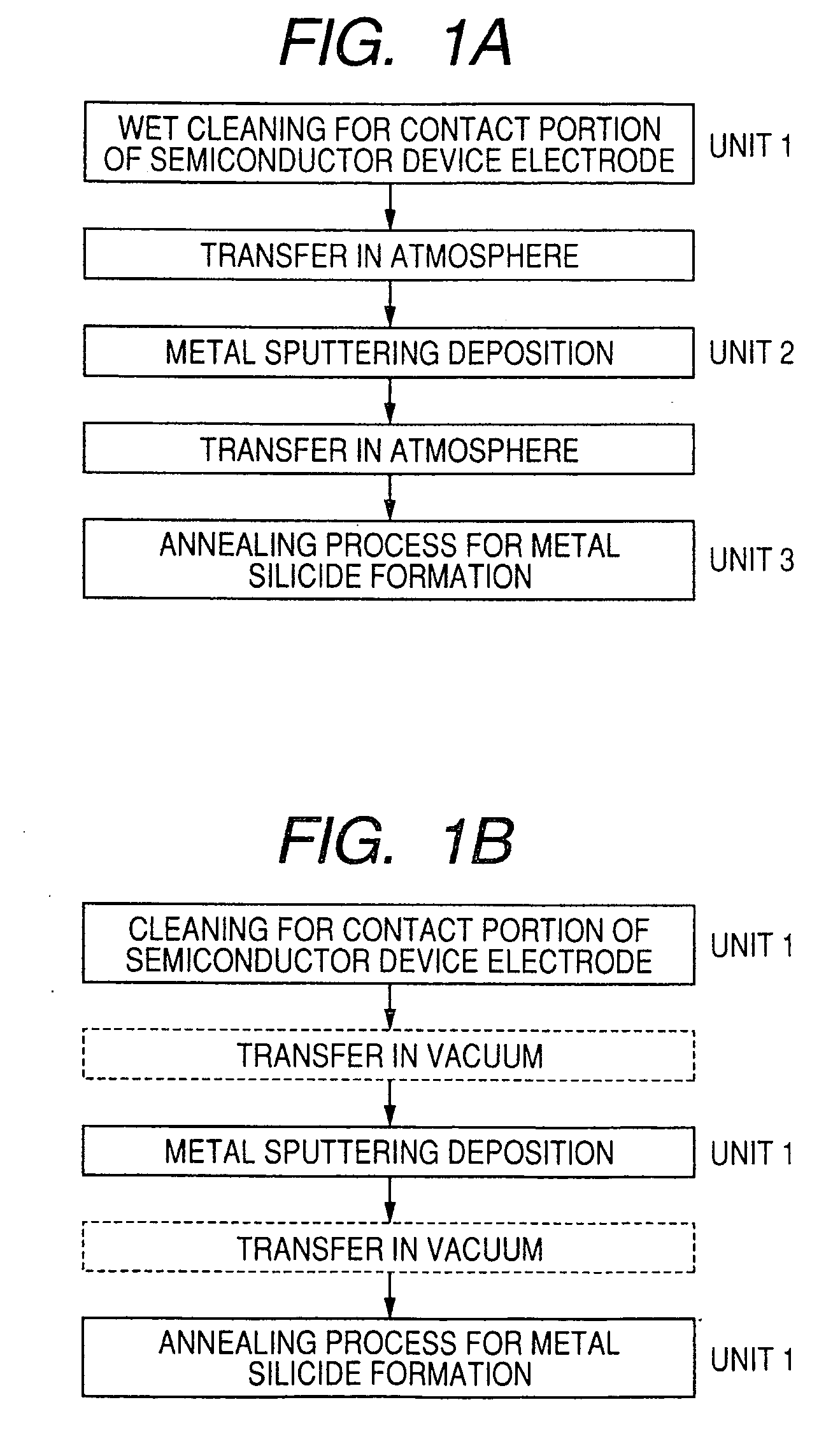
Consequently, the
wet cleaning is limited, and as shown in FIG. 1B, a
dry cleaning that performs deposition pretreatment of the semiconductor substrate in vacuum is required.
However, if the gas is turned into
plasma, since it not only contains a radicalized
fluorine gas, but also contains an ionized
fluorine gas, when the native oxide film of the
substrate surface is removed,
etching advances up to the
substrate surface, thereby causing a problem that unevenness arises on the surface.
In this case, the defects in Si are immediately formed with the oxide film, and non-coupled hands of Si are easily adsorbed with contaminated materials Hence, a problem of damages to the device arises.
Further, because two modules are used, it takes a long time before the silicide is formed.
On the other hand, in the chemical
plasma and physical
plasma cleaning, since
etching advances not only to the native oxide film, but also to the substrate surface, there is a problem that the
contact resistance causing unevenness on the surface is not sufficiently reduced.
Further, in the surface where the impurities such as B, P, and As are doped on a IV group semiconductor, there is a problem that the re-oxidation and roughness of the surface after the
surface cleaning deteriorate due to dependency on the impurity concentration.
Further, since the forming process of the
metal silicide film is easily affected by the temperature, when substrate heating is used for the removal of the native oxide film prior to the pre-deposition, the
deposition temperature of the metal material is increased, and this causes a problem that the
diffusion and composition change of the metal material occur and the metal silicide film having the desired characteristic is not obtained.
Further, when the substrate heating is used for the removal of the native oxide film prior to the deposition, if an attempt is made to reduce the
deposition temperature of the metal material in order to obtain the metal silicide film having the desired characteristic, a problem arises that a cooling unit or a plurality of processes such as a
cooling time are required, and the
processing time becomes long and the cost on the device production is increased.

