

Quinone Compound, Electrophotographic Photoconductor and Electrophotographic Apparatus
a photoconductor and compound technology, applied in the field of quinone compound, can solve the problems of increased susceptibility to physical and chemical deterioration, insufficient sensitivity of single-layer photoconductors for application to high-speed apparatuses, and damage to the environment, and achieve the effect of practicable surface potential
- Summary
- Abstract
- Description
- Claims
- Application Information
AI Technical Summary
Benefits of technology
Problems solved by technology
Method used
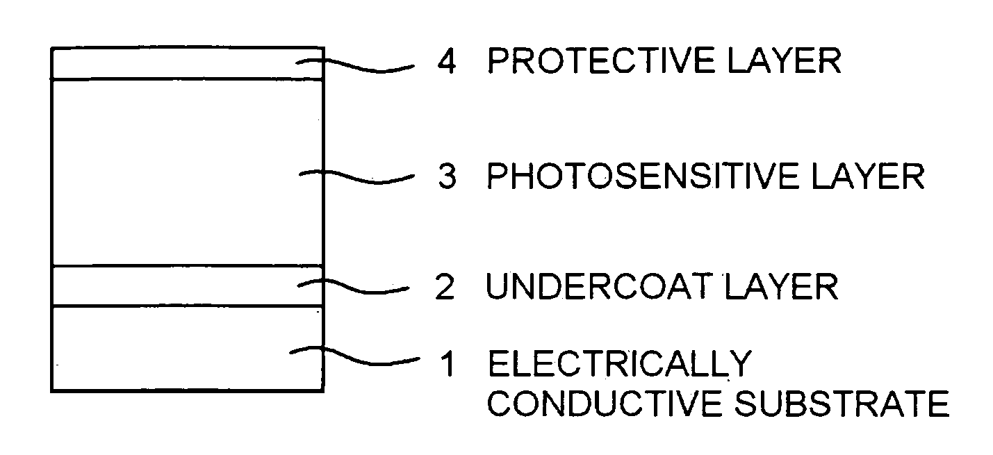
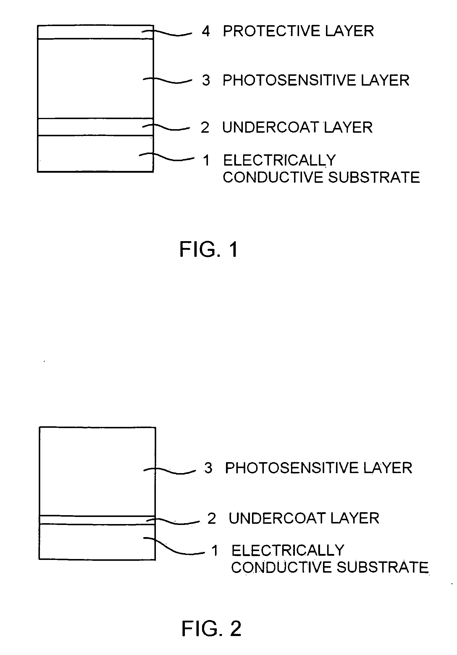
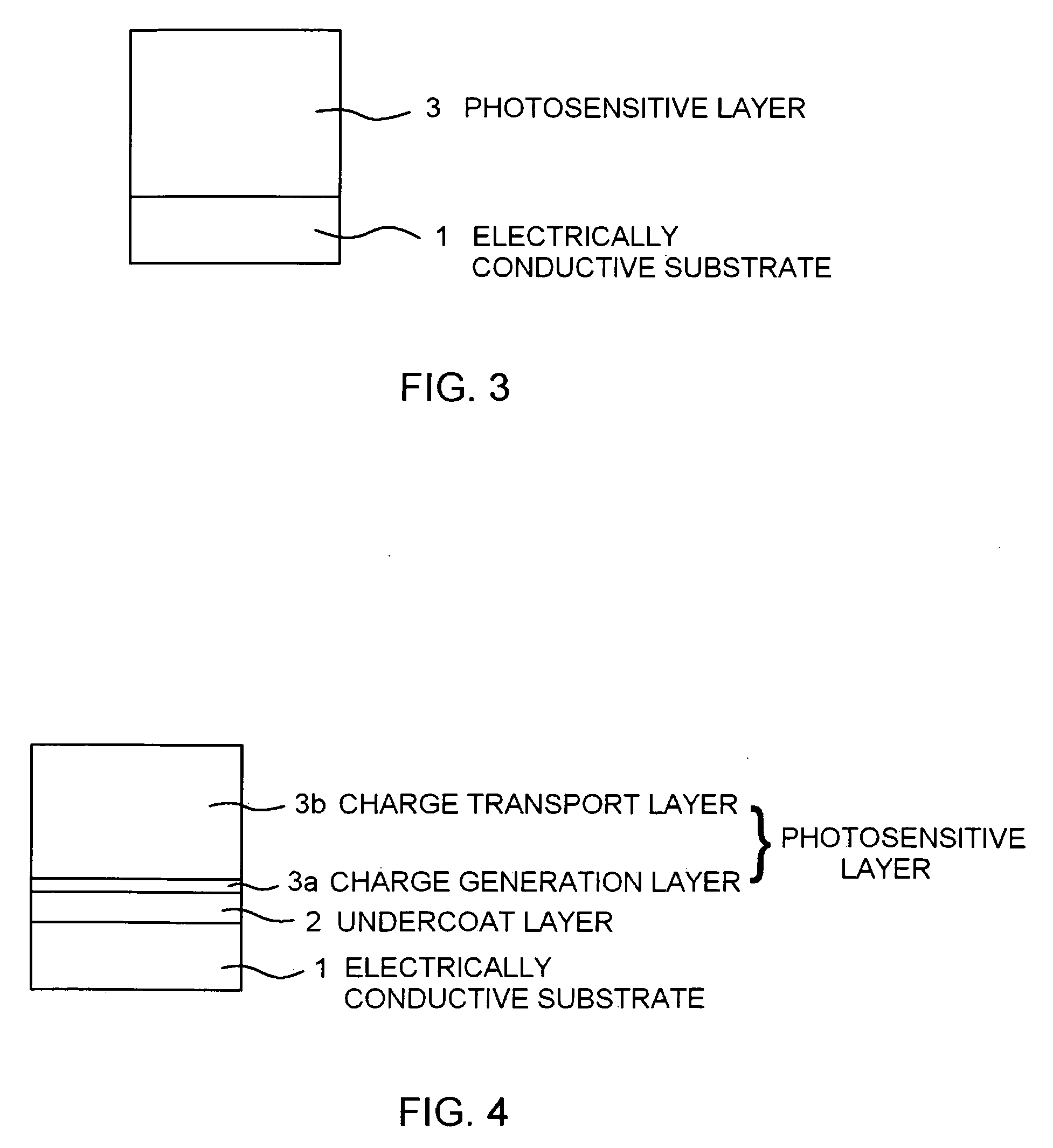
Image

Examples
synthesis example 1
Synthesis of Compound of Specific Example (I-8)
(1) Synthesis of Bishydrazone
[0087]100.0 mL of concentrated hydrochloric acid were added to 28.0 g (124.2 mmol) of stannous chloride dihydrate and 737.3 mg (6.2 mmol) of tin followed by heating and stirring until the tin dissolved. 100.0 mL of concentrated hydrochloric acid were then added to 10.0 g (31.1 mmol) of 2,2′,5,5′-tetrachlorobenzidine followed by stirring for 1 hour at room temperature until amine crystals formed a slurry. After cooling to -20° C, 18 ml of an aqueous solution of 4.5 g (65.2 mmol) of sodium nitrite were dropped in over the course of 30 minutes followed by stirring for 1 hour. The above-mentioned stannous chloride solution was cooled to 5° C. and dropped into a diazoation solution over the course of 30 minutes. Following completion of addition, the solution was stirred for 1 hour, the resulting solid was filtered out with a glass filter and then washed with 100 ml of 1% aqueous hydrochloric acid solution. This w...
synthesis example 2
Synthesis of Compound of Specific Example (I-21 )
(1) Synthesis of Bishydrazone
[0095]Synthesis was carried out in the same manner as Synthesis Example 1-(1) using 10.0 g (31.2 mmol) of 2,2′-bistrifluoromethylbenzidine to obtain 24.0 g (30.7 mmol) of the target compound.
[0096]Yield: 98.2%, mp: 223 to 226° C.
[0097]1H-NMR (500 MHz, CDCl3): δ1.48 (s,36H), δ5.38 (s,2H), δ7.18 (d,J=8.5 Hz,2H), δ7.23 (dd,J=8.5 Hz,2.4 Hz,2H)), δ7.42 (d,J=2.4 Hz,2H), δ7.51 (s,4H), δ7.61 (brs,2H), δ7.72 (s,2H)
[0098]MS (m / z): 783, 551, 319, 190
(2) Synthesis of Compound of Specific Example (I-21)
[0099]Synthesis was carried out in the same manner as Synthesis Example 1-(2) using 5.00 g (6.39 mmol) of the hydrazone compound obtained in Synthesis Example 2-(1) to obtain 3.18 g (4.08 mmol) of the target compound.
[0100]Yield: 63.9%, mp: 149 to 154° C.
[0101]1H-NMR (500 MHz, CDCl3): δ1.37 (s,18H), δ1.39 (s,18H), δ7.16 (d,J=2.3 Hz,2H), δ7.50 (d,J=8.2 Hz,2H), δ7.73 (s,2H), δ8.01 (dd,J=2.3 Hz,8.2 Hz,2H), δ8.33 (s,2H), δ8....
synthesis example 3
Synthesis of Compound of Specific Example (I-28)
[0103](1) Synthesis of 2,2′-bistrifluoromethyl-5,5′-dibromobenzidine
[0104]20.0 g (62.5 mmol) of 2,2′-bistrifluoromethylbenzidine were dissolved in 100 mL of ethanol in a nitrogen atmosphere followed by dropping in 21.0 g (131.2 mmol) of bromine over the course of 1 hour while cooling with ice. After stirring for 1 hour at room temperature, toluene was added followed by washing the organic phase three times with water and then washing two times each with saturated aqueous sodium bicarbonate solution and water. Following concentration, the concentrate was recrystallized from hexane / toluene to obtain 11.5 g (24.1 mmol) of the target compound.
[0105]Yield: 38.5%, mp: 154 to 157° C.
[0106]1H-NMR (500 MHz, CDCl3): δ4.33 (s,4H), δ7.05 (s,2H), δ7.32 (s,2H)
MS (m / z): 478, 298
(2) Synthesis of Bishydrazone
[0107]Synthesis was carried out in the same manner as Synthesis Example 1-(1) using 5.0 g (10.5 mmol) of 2,2′-bistrifluoromethyl-5,5′-dibromobenzi...
PUM
| Property | Measurement | Unit |
|---|---|---|
| thickness | aaaaa | aaaaa |
| thickness | aaaaa | aaaaa |
| thickness | aaaaa | aaaaa |
Abstract
Description
Claims
Application Information