Microbolometer pixel and fabrication method utilizing ion implantation

Active Publication Date: 2010-09-30
BAE SYST INFORMATION & ELECTRONICS SYST INTERGRATION INC
View PDF13 Cites 9 Cited by
  • Summary
  • Abstract
  • Description
  • Claims
  • Application Information

AI Technical Summary

Benefits of technology

[0013]An added benefit is that replacing the prior art metallization process with ion implantation conversion improves device performance by increasing the sensing area of the bridge (smaller metallized area required), smaller thermal mass of the bridge (no insulating dielectric or added metal), higher TCR of the mixed phase vanadium oxide compared to an alloy like NiCr (better sensitivity), and lower thermal conductance of the mixed phase vanadium oxide in the leg. In other words, the converted area for the detector contact occupies less of the sensing portion of the bridge, has a higher TCR than metallization, is without added me

Problems solved by technology

However, the VOx used in the pixel bridge cannot be used as the electrical trace because it is not metallic; i.e., its electrical resistance is too high.
Each step arising from the need for the added metallization negatively affects the cost and schedule of building microbolometers, and increases the chance of lower yield due to loss of pixels and die from the multiple processing steps.
In addition, as state of the art pushes pixels to become ever smaller and the films thinner, these processing steps become more difficult to scale for smaller geometries.
For example, continuous step coverage of the thin metal over the dielectric into the detector contact area becomes a more significant issue if the topology of the pixel is not minimized.
Back-sputter

Method used


Image

  • Microbolometer pixel and fabrication method utilizing ion implantation
  • Microbolometer pixel and fabrication method utilizing ion implantation
  • Microbolometer pixel and fabrication method utilizing ion implantation

Examples


Embodiment Construction

[0031]A pixel and a process for manufacturing a microbolometer pixel using ion implantation according to the present invention is described as follows.

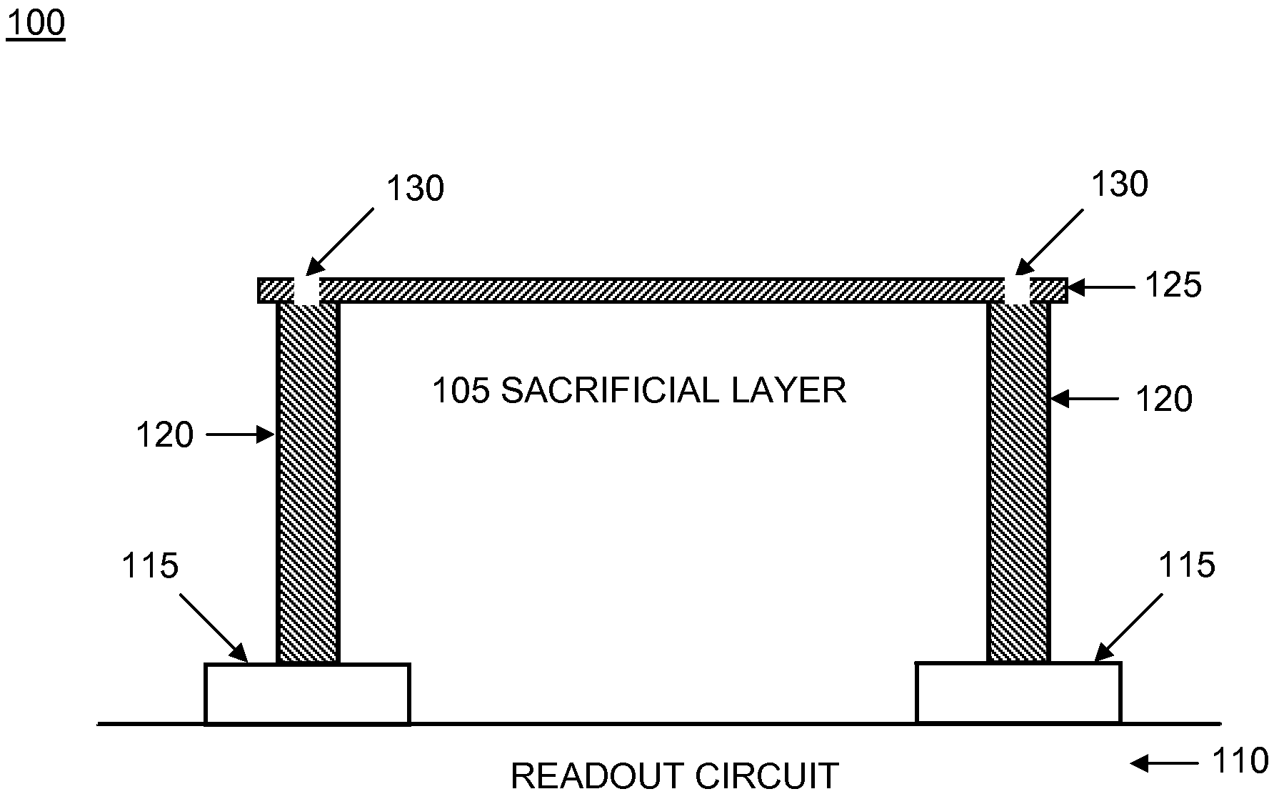
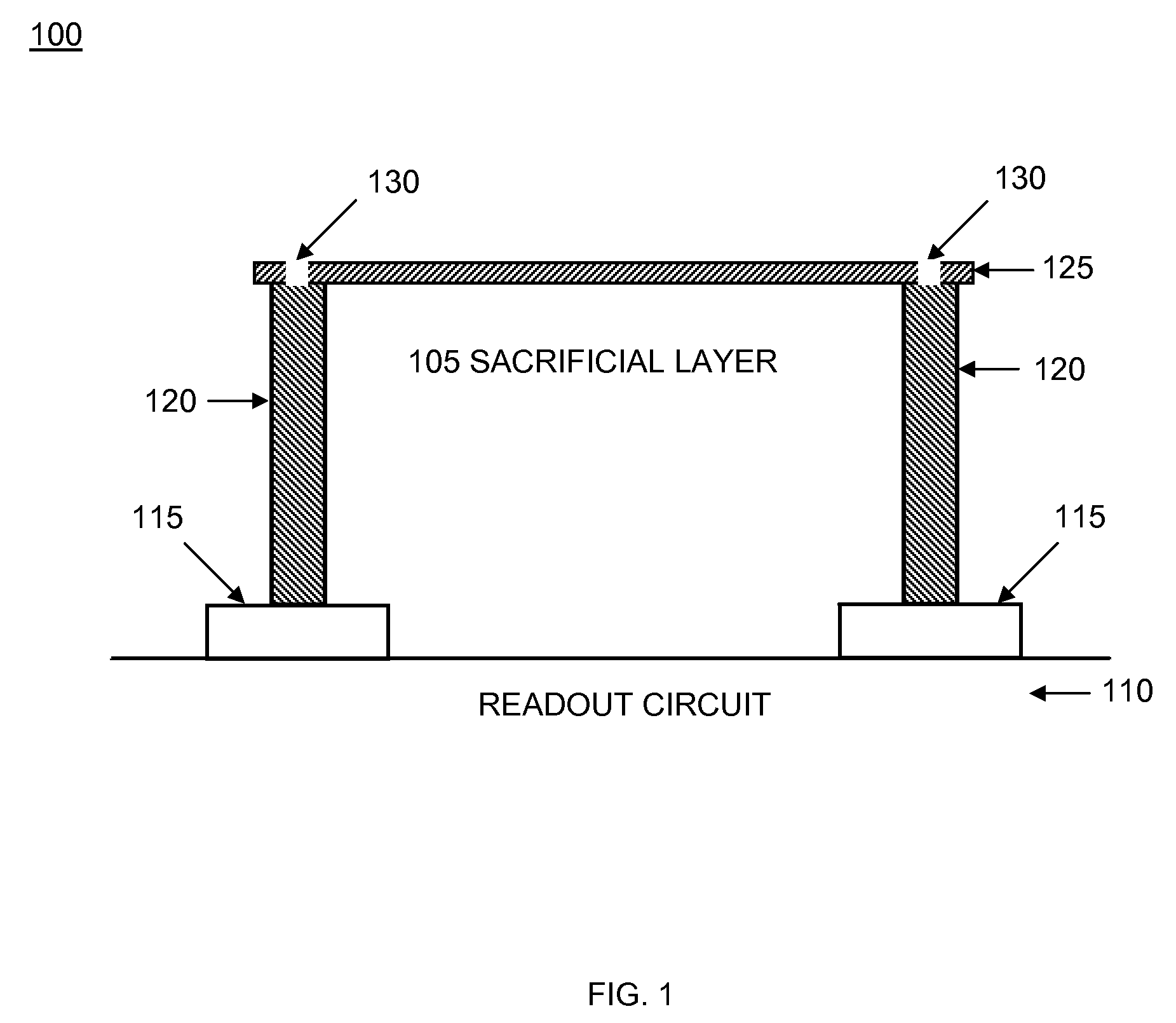
[0032]FIG. 1 is a cross section view of the initial fabrication steps 100 depicting elements around sacrificial layer 105. Underlying readout integrated circuit (ROIC) 110 has metalized pads 115 providing electrical connection to metal filled posts 120. First dielectric layer 125 is adjacent metal filled posts 120. Contact openings 130 penetrate first dielectric 125 to metal posts 120.

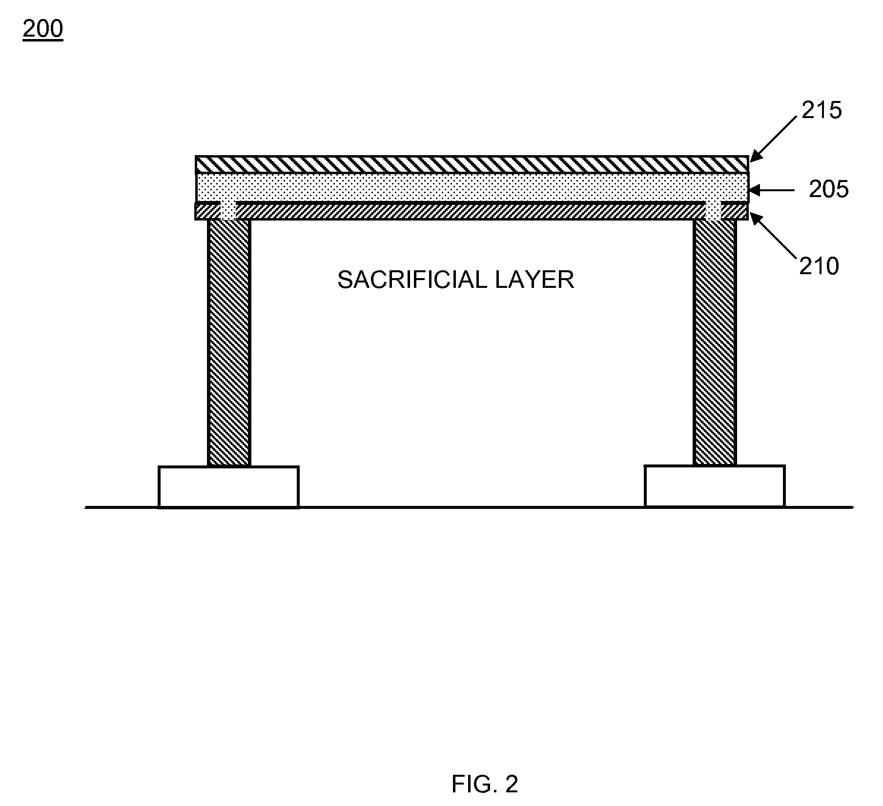
[0033]FIG. 2 is a cross section view of vanadium oxide VOx and protective dielectric film deposition steps 200. Vanadium oxide VOx layer 205 is deposited on dielectric such as silicon nitride 210. The original VOx layer thickness is typically 400 to 1500 Angstroms. Protective second dielectric layer 215 is deposited on VOx layer 205. These layers are for the formation of the suspended pixel.

[0034]FIG. 3 is a cross section view of photoresist deposition a...


PUM


Abstract

A microbolometer pixel and a reduced-step process for manufacturing it comprising the step of ion implantation of vanadium oxide whereby VOx is converted to a low resistivity mixed phase vanadium oxide (VOx/V2O3/VO/V) in the leg, metallized support post, and detector contact areas. Masking maintains high temperature coefficient of resistance (TCR) VOx in the sensing portion of the pixel bridge region. The implanted area resistivity and TCR can be controlled by ion implantation dose and energy.

Description

FIELD OF THE INVENTION[0001]The present invention relates to microbolometers and more particularly to microbolometer pixels fabricated utilizing ion implantation.BACKGROUND OF THE INVENTION[0002]One type of an infrared detector consists of a microbolometer responsive to the heat energy of infrared radiation. These microbolometers are typically grouped on a single substrate into an array of microbolometers. Microbolometer construction includes a sensor portion or pixel bridge, readout circuitry, and interconnections. In certain microbolometers, the pixel bridge is formed from an oxide of vanadium (VOx), which has a high temperature coefficient of resistance (TCR) making it an excellent IR sensing material.[0003]A conductive path is needed to provide the electrical connection between the vanadium oxide (VOx) of the pixel bridge and the underlying readout integrated circuit (ROIC). Part of this connection is a metal trace leading from the pixel bridge to the metal support structure. Th...

Claims


Application Information

Patent Timeline
IPC IPC(8): G01J5/00A61N5/00
CPCG01J5/023G01J5/024G01J5/046G01J5/20H01L31/09H01C17/06H01L27/14669H01L27/14692H01C7/026
Inventor GENECZKO, JEANNIE
Owner BAE SYST INFORMATION & ELECTRONICS SYST INTERGRATION INC
Why Eureka
Try Eureka