N-type conductive aluminum nitride semiconductor crystal and manufacturing method thereof

a technology of conductive aluminum nitride and semiconductor crystal, which is applied in the direction of crystal growth process, polycrystalline material growth, chemically reactive gas, etc., can solve the problems of deterioration of device properties, inability to efficiently produce aln single crystal film having enough thickness to obtain self-supporting substrate, and inability to produce aln single crystal film having enough thickness to achieve the effect of self-supporting substrate, good electric properties, and marked reduction of halogen impurities

Active Publication Date: 2010-12-23
TOKUYAMA CORP +1
View PDF13 Cites 17 Cited by
  • Summary
  • Abstract
  • Description
  • Claims
  • Application Information

AI Technical Summary

Benefits of technology

[0008]The present inventors made every effort for the purpose of obtaining the n-type conductive aluminum nitride semiconductor crystal which has little content of halogen impurities and has good electric properties by the HVPE method. Consequently, we found that not only the effect of increasing the growing rate was observed, but also the crystal quality, i.e. the dislocation density contained in the crystal was reduced, further, content of halogen impurities was markedly reduced in the case of firstly forming the AlN crystal layer followed by secondly forming the n-type conductive aluminum nitride semiconductor crystal layer thereon instead of forming the n-type conductive aluminum nitride semiconductor crystal directly on the substrate and in the case of making the substrate temperature at 1,200° C. or more when forming the crystal layer. Then we examine physical properties of the n-type conductive aluminum nitride semiconductor crystal obtained in that way to find that the n-type conductive aluminum nitride semiconductor crystal is characterized in that it does not substantially absorb the light which has the energy of not more than 5.9 eV. And this finding has lead to completion of the present invention.

Problems solved by technology

In such n-type electrode structure wherein the electric current flows along the n-type conductive aluminum nitride semiconductor crystal layer and the current pass becomes laterally elongated, the heat resulting in deterioration of the device properties is generated by the increased electric resistance corresponding to the elongation of the current pass.
Applying the above described method disclosed in JP-A 2000-91234 to the AlN, however, it was found that homogeneity of the AlN which grows on the substrate was markedly deteriorated because the reaction between aluminum halide used as an aluminum source and ammonia gas used as a nitrogen source is very fast compared to the reaction between gallium halide and ammonia.
It was also found that the AlN single crystal film having enough thickness to obtain the selfsupporting substrate could not be produced efficiently by the method described in JP-A 2000-91234 because the highest crystal growth rate to obtain a single crystal at the temperature of 1,100° C. was around a few μm / h.
When containing halogen impurities, there are concerns about reduction of the durability as well as reduction of the electric properties.

Method used


Image

  • N-type conductive aluminum nitride semiconductor crystal and manufacturing method thereof
  • N-type conductive aluminum nitride semiconductor crystal and manufacturing method thereof

Examples


example 1

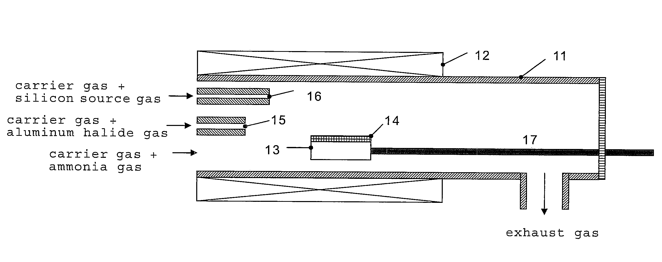
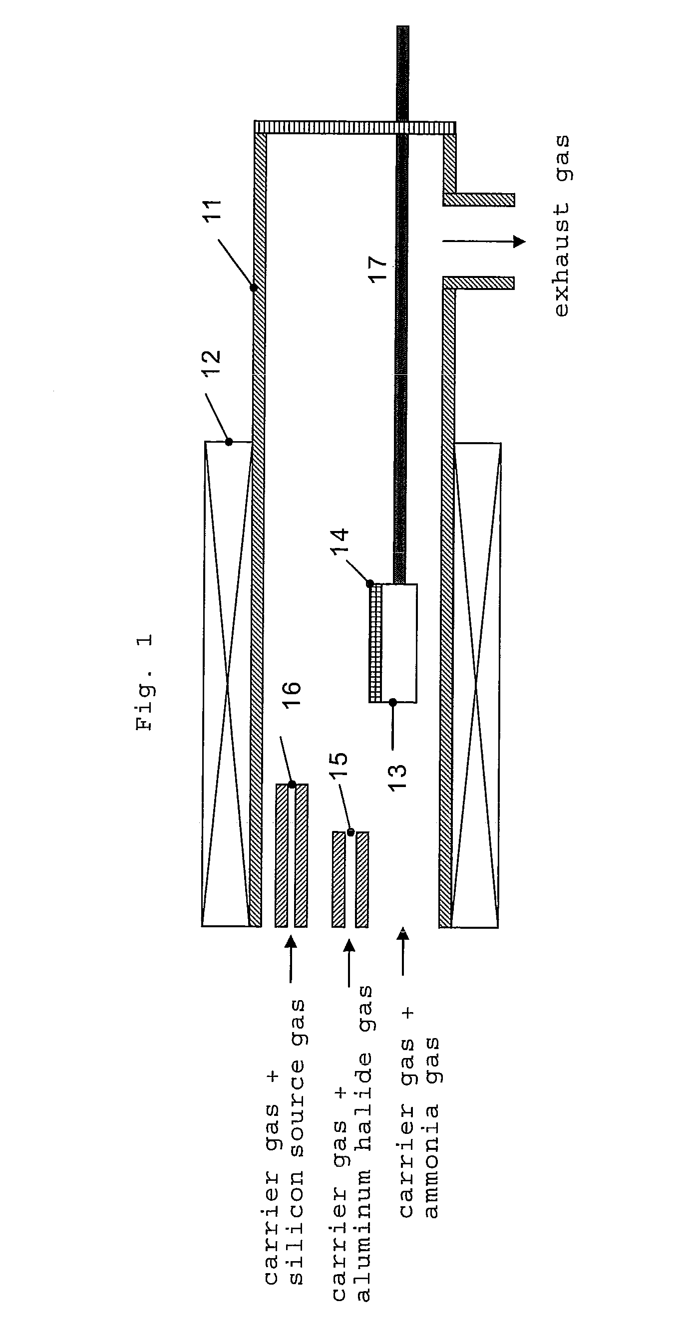
[0070]In this example, the n-type conductive aluminum nitride semiconductor crystal was grown using the reaction tube shown in the FIG. 1. In the example, the aluminum trichloride gas was generated by reacting the metal aluminum set upstream the reaction tube with hydrogen chloride gas at 500° C. Also, the sapphire (0001) substrate set on the susceptor could be heated to 1,200° C. or more by supplying the electric power from the outside to the carbon heating element using a resistance heating furnace as the external heating apparatus as well as using a susceptor consisted of the pyrolytic boron nitride which has a carbon heating element inside the reaction tube. Further, the aluminum trichloride gas used as the aluminum source gas and ammonia gas used as the nitrogen source gas were reacted to grow aluminum nitride. As the silicon source, SiCl4 was used.

[0071]First, a sapphire (0001) substrate was set on the susceptor in the reaction tube, in the normal pressure, 300 sccm of hydroge...

example 2

[0075]In this example, all procedures and conditions were the same in growing the n-type conducting aluminum nitride semiconductor crystal except that the quantity of SiCl4 supplied during growing the second stage i.e. growing the n-type conducting aluminum nitride semiconductor crystal was 0.005 times the partial pressure of aluminum trichloride gas supplied.

[0076]The film thickness of the grown n-type conducting aluminum nitride semiconductor crystal was 5.7 μm and the growing rate was 11.4 μm / h. The silicon concentration measured by the secondary ion mass spectrometer was 1×1020 cm−3, the oxygen concentration was 1×1019 cm−3, and the chlorine concentration was not more than 1×1018 cm−3. The dislocation density was calculated according to the transmission electron microscope and it was 1×1010 cm−2. The resistivity measured by the noncontact resistivity measuring apparatus was 38 Ω·cm. When observing the surface by the atomic force microscope, it was smoothed to the extent that the...

example 3

[0077]The aluminum nitride epitaxial layer which has the thickness of 130 μm was laminated on the silicon substrate using the reaction tube shown in FIG. 1 based on the method disclosed in “Embodiment 1” of JP-A 2005-252248, then it was immersed in a etchant prepared such that 50% of hydrofluoric acid, concentrated nitric acid, 98% of acetic acid and the pure water were 1:2:1:4 by volume ratio to dissolve only the silicon base which was the primary substrate, with result that the aluminum nitride selfsupporting substrate was obtained.

[0078]Subsequently, all the same procedures and conditions were used to grow the n-type conducting aluminum nitride semiconductor crystal except that the above aluminum nitride selfsupporting substrate was used instead of the sapphire (0001) substrate used in the Example 1.

[0079]The film thickness of the grown n-type conducting aluminum nitride semiconductor crystal was 5.2 μm and the growing rate was 10.4 μm / h. The silicon concentration measured by the...


PUM

PropertyMeasurementUnit
thicknessaaaaaaaaaa
temperatureaaaaaaaaaa
thicknessaaaaaaaaaa

Abstract

This invention provides a selfsupporting substrate which consists of a n-type conductive aluminum nitride semiconductor crystal and is useful for manufacturing the vertical conductive type AlN semiconductor device.The n-type conductive aluminum nitride semiconductor crystal, by which the selfsupporting substrate is made up, contains Si atom at a concentration of 1×10¹⁸ to 5×1020 cm−3, is substantially free from halogen atoms, and substantially does not absorb the light having the energy of not more than 5.9 eV. The selfsupporting substrate can be obtained by a method comprising the steps of forming an AlN crystal layer on a single crystal substrate such as a sapphire by the HVPE method, preheating the obtained substrate having the AlN crystal layer to a temperature of 1,200° C. or more, forming a second layer consisting of the n-type conductive aluminum nitride semiconductor crystal is formed on the AlN crystal layer in high rate by the HVPE method and separating the second layer from the obtained laminate.

Description

FIELD OF THE INVENTION [0001]The present invention relates to an n-type conductive aluminum nitride semiconductor crystal doped with Si atom and manufacturing method thereof.BACKGROUND OF THE INVENTION [0002]Aluminum nitride (AlN) is expected to be a material for ultraviolet light emitting device since it has as great as 6.2 eV of the forbidden band gap and it is a directly transmitting-type semiconductor.[0003]In order to form a semiconductor device including a light emitting device, it is necessary to form a n-type semiconductor layer jointed electrically to a n-electrode, a p-type semiconductor layer jointed electrically to a p-electrode and a laminated structure therebetween, where in the laminated structure comprises a clad layer, an active layer and the like. For the semiconductor device, it is required in view of light emitting efficiency that each of those layers consist of a crystal having high crystallinity, that is, having low density of point defect or dislocation and th...

Claims


Application Information

Patent Timeline
Patent Type & Authority Applications(United States)
IPC IPC(8): H01L29/06H01L29/20H01L21/203H01L33/00
CPCC30B25/02C30B29/403H01L21/02389H01L21/02403H01L33/007H01L21/02458H01L21/0254H01L21/02576H01L21/0262H01L21/0242H01L33/02
Inventor KOUKITU, AKINORIKUMAGAI, YOSHINAONAGASHIMA, TORUTAKADA, KAZUYAYANAGI, HIROYUKI
Owner TOKUYAMA CORP
Why Eureka
Try Eureka