In-ga-zn-sn type oxide sinter and target for physical film deposition

a technology of sintering body and target, which is applied in the direction of conductive materials, non-conductive materials with dispersed conductive materials, diaphragms, etc., can solve the problems of low productivity and high cost, and it is impossible to obtain a target with a sufficiently low resistance, etc., to achieve stable discharge, increase the area, and facilitate production

Active Publication Date: 2011-10-27
IDEMITSU KOSAN CO LTD
View PDF0 Cites 38 Cited by
  • Summary
  • Abstract
  • Description
  • Claims
  • Application Information

AI Technical Summary

Benefits of technology

[0079]The gate insulating film may have a structure in which two or more different layers are stacked. The gate insulating film may be crystalline, polycrystalline or amorphous. However, the gate insulating film is preferably polycrystalline or amorphous since a polycrystalline or amorphous film is easily produced on the industrial basis.
[0080]There are no particular restrictions on the material of a source electrode or a drain electrode. Within a range which does not impair the advantageous effects of the invention in this embodiment, metals or alloys thereof or oxide conductor materials, which are generally used, can be arbitrary selected.
[0081]As the sputtering method for forming an active layer, DC sputtering methods, DC magnetron sputtering methods, AC sputtering methods, AC magnetron sputtering methods, RF sputtering methods, RF magnetron sputtering methods; opposing target sputtering methods, cylindrical target sputtering methods, ECR sputtering methods or the like can be used. As the vacuum vapor deposition method, resistance heating methods, electron beam heating methods, pulse laser deposition (PLD) methods or the like can be used. As the ion plating method, ARE methods and HOPE methods can be used. As the CVD method, thermal CVD methods and plasma CVD methods can be used.
[0082]Of these methods, DC magnetron sputtering methods or AC magnetron sputtering methods which are inexpensive, capable of increasing the area and exhibit stable discharge are preferable for industrialization. DC magnetron sputtering methods are particularly preferable. In addition, co-sputtering, reactive sputtering, or RF-superimposed DC sputtering may be used.
[0083]When sputtering methods are used, the ultimate pressure is normally 5×10⁻² Pa or less. The reason therefor is that, if the ultimate pressure is larger than 5×10⁻² Pa, mobility may be lowered due to impurities in an atmospheric gas.
[0084]In order to avoid such disadvantages more effectively, the ultimate pressure is preferably 5×10⁻³ Pa or less, more preferably 5×10⁻⁴ Pa or less, further preferably 1×10⁻⁴ Pa or less, with 5×10⁻⁵ Pa or less being particularly preferable.

Problems solved by technology

Due to the large number of steps, this target has disadvantages of low productivity and high cost.
That is, it is impossible to obtain a target with a sufficiently low resistance.
However, no improvement has been made on the steps, and targets are currently produced by conventional production steps.
Accordingly, these compounds are defective to be used in a sputtering target.
In addition, a problem occurs that, when sputtering (DC sputtering, for example) is conducted using an IGZO sputtering target, a compound shown by InGaO3(ZnO)m is grown extraordinary to cause abnormal discharge, resulting in the formation of a defective film.
Further, the resulting oxide film has poor resistance to chemicals, and hence, is dissolved in a PAN (phosphoric acid-acetic acid-nitric acid)-based etching solution which is used in etching for metal wires.
As a result, when producing a thin film transistor or the like using a semiconductor film, restrictions are imposed on the structure or the process.

Method used


Image

  • In-ga-zn-sn type oxide sinter and target for physical film deposition
  • In-ga-zn-sn type oxide sinter and target for physical film deposition
  • In-ga-zn-sn type oxide sinter and target for physical film deposition

Examples


example 1

(1) Oxide Sintered Body

[0090]As the raw material powder, indium oxide powder with a specific surface area of 6 m2 / g, gallium oxide powder with a specific surface area of 6 m2 / g, zinc oxide powder with a specific surface area of 3 m2 / g and tin oxide powder with a specific surface area of 6 m2 / g were weighed such that the weight ratio became 51:15:17:17 (atomic ratio of metal atoms: 0.43:0.19:0.25:0.13), and the resulting mixture was mixed and pulverized by means of a wet stirred medium mill. Zirconia beads with a diameter of 1 mm were used as the medium.

[0091]As compared with the specific surface area of the raw material powder mixture, the specific surface area of the powder was increased by 2 m2 / g after pulverization. Then, the powder was dried by means of a spray dryer.

[0092]This powder mixture was filled in a mold and then subjected to pressure molding by means of a cold pressing machine. Further, while circulating oxygen, the powder was sintered in an oxygen atmosphere at a high...

example 2

[0117]An oxide sintered body was obtained in the same manner as in Example 1, except that the indium oxide powder, gallium oxide powder, zinc oxide powder and tin oxide powder were mixed at 42:30:14:14 in weight ratio.

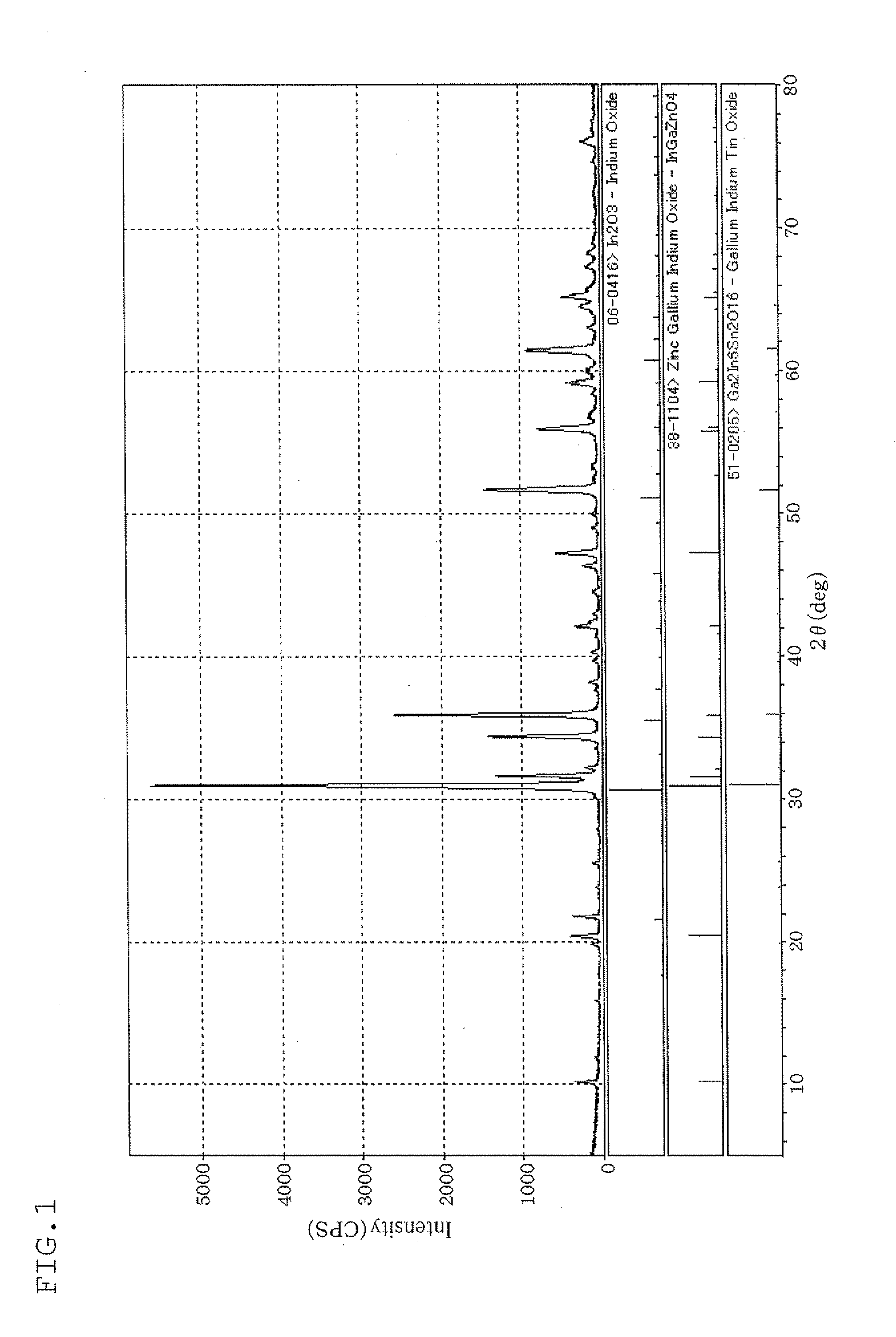
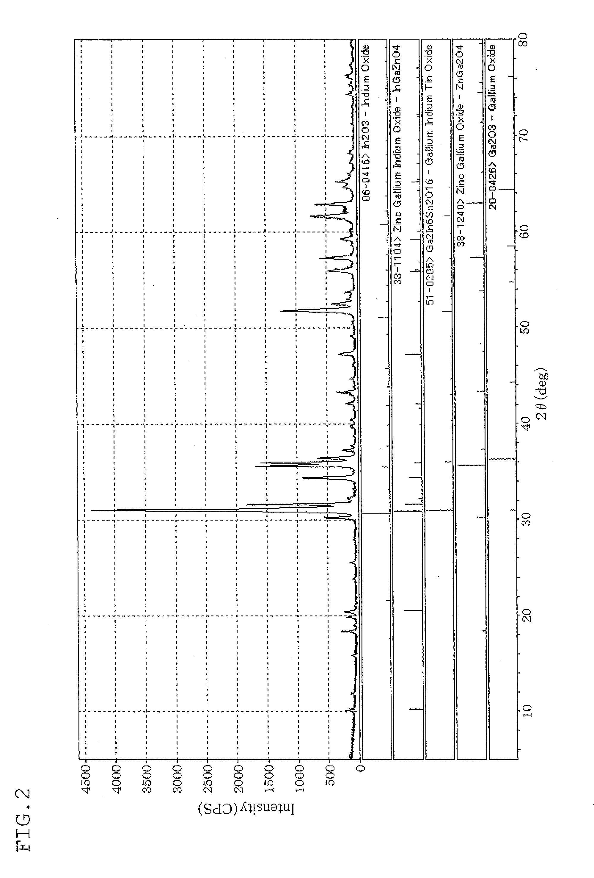
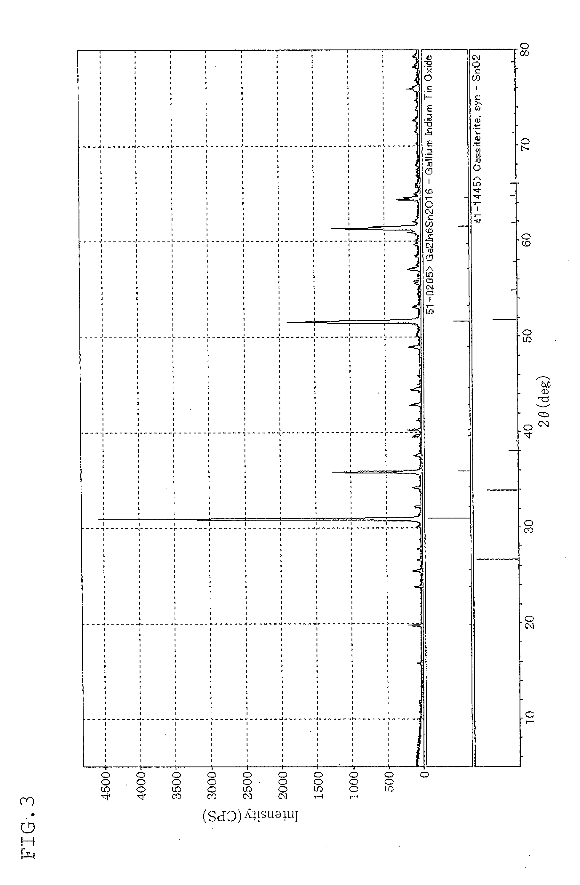
[0118]This sintered body was analyzed by X-ray diffraction. FIG. 2 is an X-ray diffraction chart of the sintered body. From this chart, it could be confirmed that this sintered body contained as a main component a compound shown by Ga2In6Sn2O16 and also contained compounds shown by In2O3, Ga2O3 or the like.

[0119]The bulk resistance of this sintered body was 4 mΩcm.

[0120]The resulting sintered body was processed into a target in the same manner as in Example 1, and an oxide semiconductor film was formed by using an RF magnetron sputtering film forming apparatus. The film forming conditions were the same as those in Example 1, and an oxide semiconductor film with a thickness of about 100 nm was formed on a glass substrate. In this example, almost no abnormal discharge wa...


PUM

PropertyMeasurementUnit
conductivityaaaaaaaaaa
particle sizeaaaaaaaaaa
resistanceaaaaaaaaaa

Abstract

An oxide sintered body including an indium element (In), a gallium element (Ga), a zinc element (Zn) and a tin element (Sn), and including a compound shown by Ga2In6Sn2O16 or (Ga,In)2O3.

Description

TECHNICAL FIELD[0001]The invention relates to an oxide sintered body and a target for physical film formation composed of an oxide sintered body.BACKGROUND ART[0002]An oxide semiconductor film composed of several metal composite oxides has a high degree of carrier mobility and visible ray transmittance. Therefore, it is used in a variety of fields including a switching element, a driving circuit element or the like for a liquid crystal display, a thin film electroluminescence display, an electrophoresis display, a moving particle display.[0003]Of these oxide semiconductor films composed of metal composite oxides, an oxide semiconductor film composed of indium oxide-gallium oxide-zinc oxide, which is called IGZO, is used most widely. In addition to IGZO, indium oxide-zinc oxide (IZO), one obtained by adding zinc oxide to tin oxide (ZTO), one obtained by adding gallium oxide to indium oxide-zinc oxide-tin oxide or the like are known. They differ from each other in easiness in producti...

Claims


Application Information

Patent Timeline
Patent Type & Authority Applications(United States)
IPC IPC(8): H01B1/02C23C14/34C23C14/08
CPCC04B35/457C04B2235/963C04B2235/3286C04B2235/3293C23C14/08C23C14/3414H01L21/02554H01L21/02565H01L21/02631C04B35/01C04B35/453C04B2235/5409C04B2235/5436C04B2235/5445C04B2235/6585C04B2235/77C04B2235/80C04B2235/3284C04B35/00H01L21/34C23C14/34
Inventor YANO, KOKIINOUE, KAZUYOSHI
Owner IDEMITSU KOSAN CO LTD
Why Eureka
Try Eureka