Sputtering Target for Oxide Thin Film and Process for Producing the Sputtering Target

a technology of oxide thin film and sputtering target, which is applied in the direction of diaphragms, metallic material coating processes, electrical devices, etc., can solve the problems of sputtering being difficult, sputtering being so difficult, and unable to achieve sputtering, etc., to achieve a high relative density, reduce bulk resistance, and the effect of stably

Inactive Publication Date: 2013-10-31
IDEMITSU KOSAN CO LTD
View PDF0 Cites 13 Cited by
  • Summary
  • Abstract
  • Description
  • Claims
  • Application Information

AI Technical Summary

Benefits of technology

[0055]The present invention provides a sputtering target having reduced bulk resistance and high relative density with retaining properties possessed by an IGZO sputtering target. By using the present invention, a sputtering target capable of reducing an abnormal electrical discharge during film-forming of an oxide thin film using a sputtering method, and also capable of film-forming continuously and stably is provided.
[0056]The present invention also provides an oxide sintered body comprising indium oxide having a bixbyite structure and a Yb2Fe3O7 structure compound represented by the formula: In2Ga2ZnO7, by controlling sintering time and composition.
[0057]An excellent oxide or TFT can be prepared by using the sputtering target of the present invention for manufacturing a semi-conductor.
[0058]The present invention provides a sputtering target having high reducing effect in bulk residence, high productivity, low cost, capable of reducing an abnormal electrical discharge during film-forming of an oxide thin film using a sputtering method, capable of film-forming continuously and stably, and capable of forming an oxide semi-conductor film having wider composition range than that of a conventional sputtering target composed of oxides of In, Ga and Zn.
[0059]By using the present invention, an oxide sintered body comprising indium oxide having a bixbyite structure and a homologous structure compound of InGaO3(ZnO)m (m is a natural number of 1 to 4) can be formed by the specific manufacturing method or the specific manufacturing condition (sintering temperature or sintering time).
[0057]An excellent oxide or TFT can be prepared by using the sputtering target of the present invention for manufacturing a semi-conductor.
[0061]The present invention provides an oxide comprising in(indium) in an amount of 49 atom % or less based on the atomicity of all the atoms included in oxides at issue other than oxide as 100 atom %, and having a crystalline structure of rare-earth oxide C type. Even though the oxide of the present invention contains low In, a sputtering target having low bulk resistance, high relative density, and high bending strength can be provided. In addition, the oxide of the present invention can provide a target which creates extremely less nodules release during sputtering, comparing it with a target containing a lot of In.

Problems solved by technology

However, when a sputtering (DC sputtering) is conducted by using the IGZO sputtering target, an abnormal electrical discharge caused by anomalous growth of the compound shown by InGaO3(ZnO)m, and thus there was a problem about defects on the obtained film.
In addition, specific resistance of the Obtained sputtering target was at least around 1×10⁻² Ωcm, this resistance is high and thus a plasma discharge is not stable, and DC sputtering was thus difficult, on top of that, a target which causes cracks during sputtering could not obtained.
In addition, the specific resistance of the target is around 1×10² Ωcm or more which is so high, the target is not appropriate for conducting DC sputtering method having good productivity.
The production process to obtain the sintered body of the compound single phase is complicated, sintering time is long, and thus a target sintered body having low cost could not be obtained.
However, the bulk resistance after the reduction was at most around 1×10⁻¹ Ωcm, and thus effect of reducing the bulk resistance was small compared to a high number of production steps thereof.
Further, the sputtering target composed of a sintered body only consisting of a compound represented by the homologues structure InGaO3(ZnO)m causes an abnormal electrical, discharge by anomalous growth during film-forming by sputtering, and thus there was a problem about defects on the obtained film.
A crystalline silicon thin film requires, for example, high temperature of 800° C. or more during crystallization, and thus it is difficult to compose it on a glass substrate or an organic material substrate.
Therefore, there are several problems, for example, the film can be formed only on an expensive substrate having high heat resistance such as a silicon wafer or quartz, and the production thereof requires a lot of energy and many steps.
A crystalline silicon thin film is limited to a top-gate structure for a devise structure of an ordinary TFT, and thus it is difficult to reduce costs by cutting a number of masks down.
However, switching speed of the film is slower than that of the crystalline film, and therefore, when the film is used for a switching device for driving a display device, displaying high-speed motion picture cannot be achieved sometimes.
Therefore, if an amorphous silicon which varies its properties by DC stress is used, there is a problem where image quality is degraded based on its long-term use.
In addition, if a crystalline silicon is used for the above usages, it becomes difficult to apply it to large-area.
There is also a problem where production cost becomes higher, because high temperature heating treatment is needed.
However, this semi-conductor layer has low mobility: about 1 cm2 / V·sec, and low ON-OFF ratio.
In addition, leak current is easy to occur, and thus it was difficult to put it into industrial, practical use.
Furthermore, many attempts were taken place for an oxide semi-conductor containing crystalline material using zinc oxide, but the following problems were present when a Min was formed by a sputtering method which is commercially and commonly used.
The obtained film has less chemical resistance, and thus process or usage environment is limited, for example, wet-etching is difficult.
Further, a film must be formed under high pressure in order to improve its properties, but film-forming speed is slow as well as 700° C. or more of high temperature is required, and thus there are problems in industrialization, in addition, TFT properties such as mobility in a bottom-gate structure is low, and thus a TFT device structure is also limited, for example, top-gate structure and 50 nm or more of thickness are required for raising its properties.
However, the homologous crystal structure has less heat stability, and thus crystalline morphology is varied based on small change of sintering temperature or sintering time.
Therefore, there are problems concerning instability in properties such as density in a target, bulk resistance, bending strength and surface roughness.
In addition, if the target is used as one for making a thin film transistor, there are problems particularly for a homologous crystal structure where properties of the transistor is significantly varied between at the start of forming a film and at the end of forming a film.A target composed of indium oxide, zinc oxide, and gallium oxide having 2.2 to 40 atom % of Ga, 50 to 90 atom % of In and 95% or more of relative density is disclosed (Patent Document 6).
However, it has been difficult to make a sintered body which can readily incorporate oxygen at the time of sintering to have low resistance.
A sputtering target composed of In2O3 (indium oxide) or containing plenty of In2O3 (indium oxide) has problems concerning that nodules (agglomerates found on a surface of the sputtering target) are easily created, that there are many particles (dusts of a sputter material found during sputtering), and that an abnormal electrical discharge during sputtering is easily occurred.
If a crystalline type other than rare-earth oxide C type, especially β-Ga2O3 is formed, problems such as crack being formed, bulk resistance being high, relative density being low, bending strength (JIS 81601) being low, difficulty in obtaining a sputtering target being uniformity in various physical properties such as a structure, are easily occurred, and thus it becomes not appropriate for applying it to a sputtering target for industrial use.

Method used


Image

  • Sputtering Target for Oxide Thin Film and Process for Producing the Sputtering Target
  • Sputtering Target for Oxide Thin Film and Process for Producing the Sputtering Target
  • Sputtering Target for Oxide Thin Film and Process for Producing the Sputtering Target

Examples


example 1

[0295]An indium oxide powder having 99.99% purity, a gallium oxide powder having 99.99% purity, and a zinc oxide powder having 99.99% purity were weighed to meet mass ratio of In2O3:Ga2O3:ZnO=61:25:14 mass %, and then mixed and ground by a wet-type medium agitating mill. Zirconia beads having 1 mmφ were used as the medium of the wet-type medium agitating mill.

[0296]After mixing and grinding each crude material, each crude material was dried by a spray dryer. The obtained mixed powder was filled in a metal mold, and then press formed by a cold press device to make a formed body.

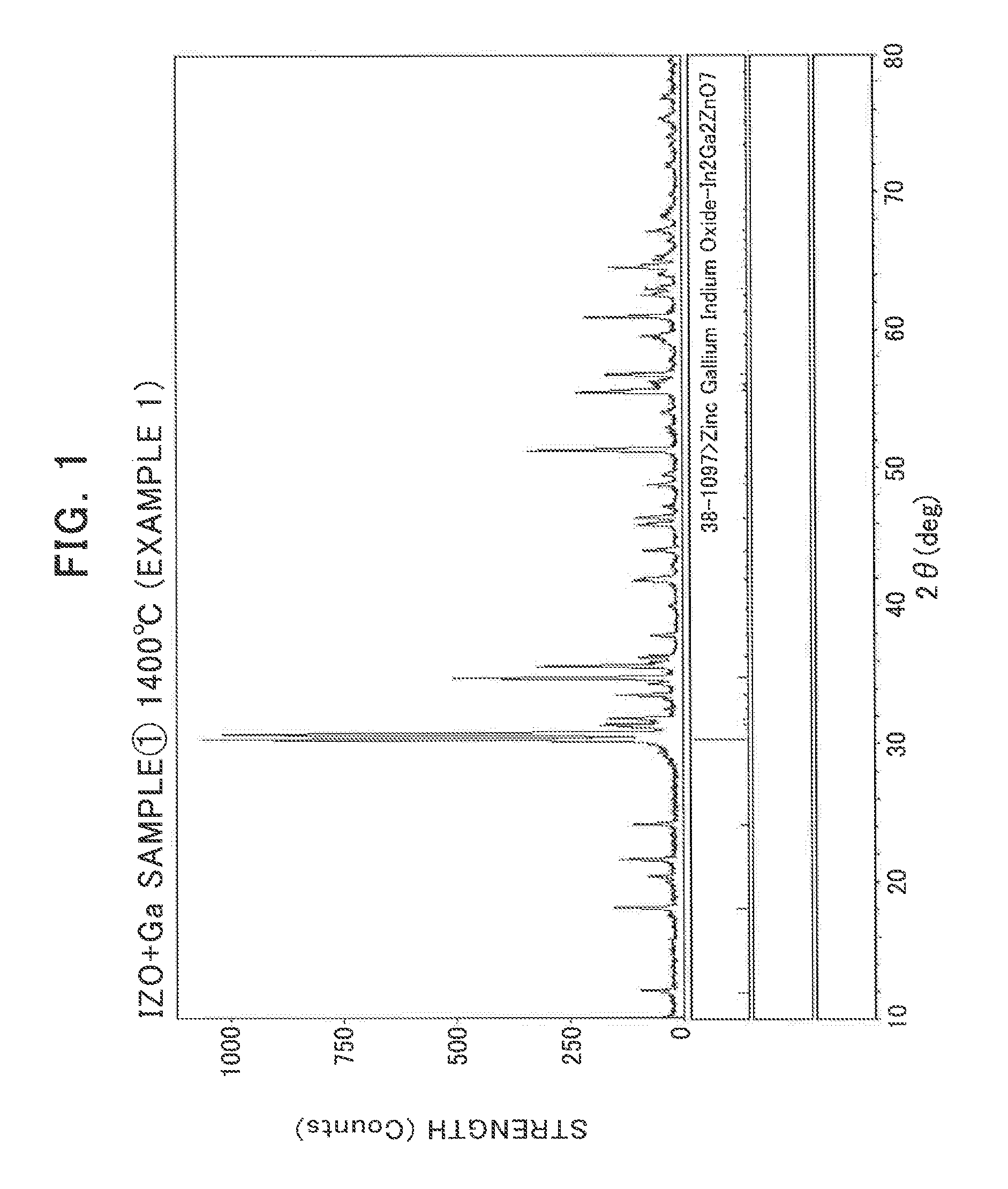
[0297]The obtained formed body was sintered under ambient atmosphere at a high temperature of 1400° C. for 2 hours. Based on the above steps, an oxide sintered body for an IGZO sputtering target having relative density of 86% was obtained. Based on X-ray diffraction, it was confirmed that a crystal of an indium oxide having a bixbyite structure and In2Ga2ZnO7 was present, X-ray diffraction pattern is shown in ...

example 2

[0300]An indium oxide powder having 99.99% purity, a gallium oxide powder having 99.99% purity, and a zinc oxide powder having 99.99% purity were weighed to meet mass ratio of In2O3:Ga2O3:ZnO=70:23:7 mass %, and then mixed and ground by a wet-type medium agitating mill. Zirconia beads having 1 mmφ were used as the medium of the wet-type medium agitating mill.

[0301]After mixing and grinding each crude material, each crude material was dried by a spray dryer. The obtained mixed powder was filled in a metal mold, and then press formed by a cold press device to make a formed body.

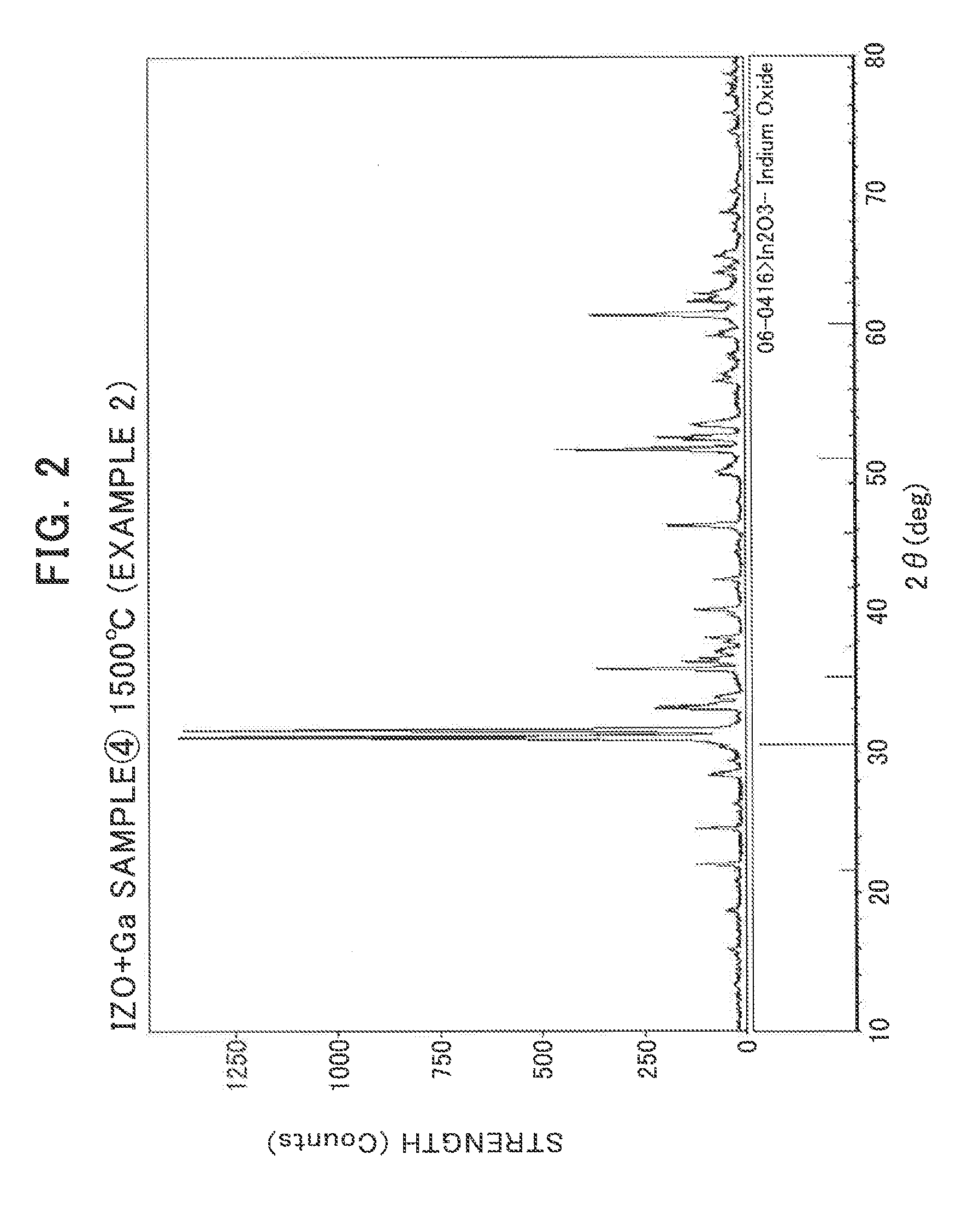
[0302]The obtained formed body was sintered under ambient atmosphere at a high temperature of 1500° C. for 2 hours. Based on the above steps, an oxide sintered body for an IGZO sputtering target having relative density of 91% was obtained. Based on X-ray diffraction, it was confirmed that a crystal of an indium oxide having a bixbyite structure and In2Ga2ZnO7 was present. X-ray diffraction pattern is shown in F...

example 3

[0304]An indium oxide powder having 99.99% purity, a gallium oxide powder having 99.99% purity, and a zinc oxide powder having 99.99% purity were weighed to meet mass ratio of In2O3:Ga2O3:ZnO=78:15:7 mass %, and then mixed and ground by a wet-type medium agitating mill. Zirconia beads having 1 mmφ were used as the medium of the wet-type medium agitating mill.

[0305]After mixing and grinding each crude material, each crude material was dried by a spray dryer. The obtained mixed powder was filled in a metal mold, and then press formed by a cold press device to make a formed body.

[0306]The obtained formed body was sintered under ambient atmosphere at a high temperature of 1400° C., for 2 hours. Based on the above steps, an oxide sintered body for an IGZO sputtering target having relative density of 83% was obtained. Based on X-ray diffraction, it was confirmed that a crystal of an indium oxide having a bixbyite structure and In2Ga2ZnO7 was present as is the case with Example 2. X-ray di...


PUM

PropertyMeasurementUnit
crystalline particle diameteraaaaaaaaaa
temperatureaaaaaaaaaa
thicknessaaaaaaaaaa

Abstract

Disclosed is a sputtering target that can suppress the occurrence of anomalous discharge in the formation of an oxide semiconductor film by sputtering method and can continuously and stably form a film. Also disclosed is an oxide for a sputtering target that has a rare earth oxide C-type crystal structure and has a surface free from white spots (a poor appearance such as concaves and convexes formed on the surface of the sputtering target). Further disclosed is an oxide sintered compact that has a bixbyite structure and contains indium oxide, gallium oxide, and zinc oxide. The composition amounts (atomic %) of indium (In), gallium (Ga), and zinc (Zn) fall within a composition range satisfying the following formula:In / (In+Ga+Zn)<0.75

Description

BACKGROUND OF THE INVENTION[0001]1. Technical Field[0002]The present invention relates to a sputtering target suitable for forming a oxide thin film and a process for producing thereof, wherein the oxide thin film is composed of an oxide sintered body which comprises indium oxide having a bixbyite structure, and a Yb2Fe3O7 structure compound represented by the formula: In2Ga2ZnO7.[0003]The present invention also relates to a sputtering target suitable for forming a oxide semi-conductor and a method for producing thereof wherein the oxide semi-conductor comprises oxides of indium (In), gallium (Ga) and zinc (Zn), and is composed of an oxide sintered body which comprises indium oxide having a bixbyite structure and a homologous structure compound InGaO3(ZnO)m (m is a natural, number of 1 to 4).[0004]The present invention relates to a sintered body having a crystal structure of rare-earth oxide C type.[0005]The present invention relates to a target having a crystal structure of rare-ea...

Claims


Application Information

Patent Timeline
Patent Type & Authority Applications(United States)
IPC IPC(8): H01L21/02H01L29/786
CPCH01L21/02565H01L29/7869C04B35/01C04B35/453C04B35/6262C04B35/62655C04B35/62695C04B37/026C04B2235/3229C04B2235/3232C04B2235/3244C04B2235/3251C04B2235/3256C04B2235/3258C04B2235/3284C04B2235/3286C04B2235/3287C04B2235/3293C04B2235/40C04B2235/5409C04B2235/5436C04B2235/6027C04B2235/652C04B2235/656C04B2235/6562C04B2235/6565C04B2235/6567C04B2235/6581C04B2235/6586C04B2235/661C04B2235/76C04B2235/761C04B2235/77C04B2235/786C04B2235/80C04B2235/96C04B2235/963C04B2235/9661C04B2237/12C04B2237/34C04B2237/407C23C14/086C23C14/3414H01L21/02554H01L21/02631Y10T428/31507B22F3/12C23C14/34
Inventor KAWASHIMA, HIROKAZUYANO, KOKIUTSUNO, FUTOSHIINOUE, KAZUYOSHI
Owner IDEMITSU KOSAN CO LTD
Why Eureka
Try Eureka