An improved method to make of fabricating ic/mram using oxygen ion implantation

a technology of oxygen ions and implantation, which is applied in the field of spinelectronic devices, can solve the problems of increasing the cost of increased write current, reducing the write current, and not having enough magnetic crystalline anisotropy to achieve thermally stable perpendicular magnetization, etc., and achieves the effect of effectively capturing oxygen ions and thicker ogls

Inactive Publication Date: 2016-06-16
T3MEMORY
View PDF10 Cites 6 Cited by
  • Summary
  • Abstract
  • Description
  • Claims
  • Application Information

AI Technical Summary

Benefits of technology

[0019]The present invention is about an improved method, over prior inventions, of fabricating integrated circuit (IC) device(s), especially magnetic random access memory (MRAM) device(s), in particular, perpendicular spin transfer torque MRAM or p-STT-MRAM device(s). Electrical isolation for IC / MRAM device(s) or cells is formed by ion implantation instead of etching and dielectric refilling. Oxygen ion implantation is used to convert the photolithography exposed areas into metal oxide dielectric matrix. An ultrathin single-layer or multiple-layer(s) of oxygen-getter, made of one or more of Mg, Zr, Y, Th, Ti, Al, and Ba, or their alloy, is / are formed to be in between sub-layers of an ADL, such as an MTJ, of active IC / MRAM device(s) especially pSTT-MRAM devices in addition to making a relatively thicker OGLs above and below ADLs, such as MTJs, to effectively capture the impinged oxygen ions. Oxygen is further confined within the core device layer by adding oxygen stopping layer below the bottom oxygen-getter. After a high temperature anneal, a uniformly distributed and electrically insulated metal oxide dielectric is formed across the middle device layer outside the photolithography protected device area, thus forming IC / MRAM cell without any physical deformation and damage at the device boundary.

Problems solved by technology

However, where a MTJ is formed as a device of a perpendicular magnetization type, the materials of the recording layer typically used in an in-plane MTJ for both high MR and low damping constant as required by low write current application normally don't have enough magnetic crystalline anisotropy to achieve thermally stable perpendicular magnetization against its demagnetization field.
Doing so, reduction in write current becomes difficult due to the fact that damping constant increases from the additional perpendicular magnetization layer and its associated seed layer for crystal matching and material diffusion during the heat treatment in the device manufacturing process.
Although a high perpendicular anisotropy is preferred in term of a high thermal disturbance resistance, an increased write current is expected as a cost.
More, even when the tunnel barrier does not immediately break down, if recording operations are repeated, the element may still become nonfunctional such that the resistance value changes (decreases) and information readout errors increase, making the element un-recordable.
Furthermore, recording is not performed unless a sufficient voltage or sufficient spin current is applied.
Accordingly, problems with insufficient recording arise before possible tunnel barrier breaks down.
However, patterning of small MTJ element leads to increasing variability in MTJ resistance and sustaining relatively high switching current or recording voltage variation in a STT-MRAM.
The MTJ patterning process becomes one of the most challenging aspects of manufacturing.
Conventional techniques utilized to pattern small dimensions in a chip, such as ion milling etching (IBE) or reactive ion etching (RIE), having been less than satisfactory when applied to magnetic tunnel junction stacks used for MRAM.
In most cases when these techniques are used, it is very difficult or almost impossible to cleanly remove etched materials without partial damages to magnetic tunnel junction properties and electric current shunting.
In a RIE etching of magnetic material, physical sputtering is still the major component which unavoidable results in the formation of re-deposited residues that can short circuit the junctions of the MTJ or create shunting channel of the MTJ, yielding high resistance variations and serious reliability issues.
Another problem of conventional patterning techniques is the degradation of the recording layer and reference layer in the MTJ, due to corrosion caused by chemical residue remaining after etching.
Exposure to reactive gases during refilling deposition of dielectrics such as silicon dioxide or silicon nitride after the MTJ etching can also cause corrosion.
After refilling of dielectric material, a chemical mechanic polishing process is required to smooth out the top surface for bit line fabrication, which introduces a big manufacturing challenging as well as high cost and further corrosion.
As the result, the formed sensor size cannot be made small enough to reduce the write current to switch the memory layer.
Also, due to the non-volatile nature of the etched magnetic materials, often the etched sensor edge got damaged with electrical shorting across the MgO barrier.

Method used


Image

  • An improved method to make of fabricating ic/mram using oxygen ion implantation
  • An improved method to make of fabricating ic/mram using oxygen ion implantation
  • An improved method to make of fabricating ic/mram using oxygen ion implantation

Examples


Embodiment Construction

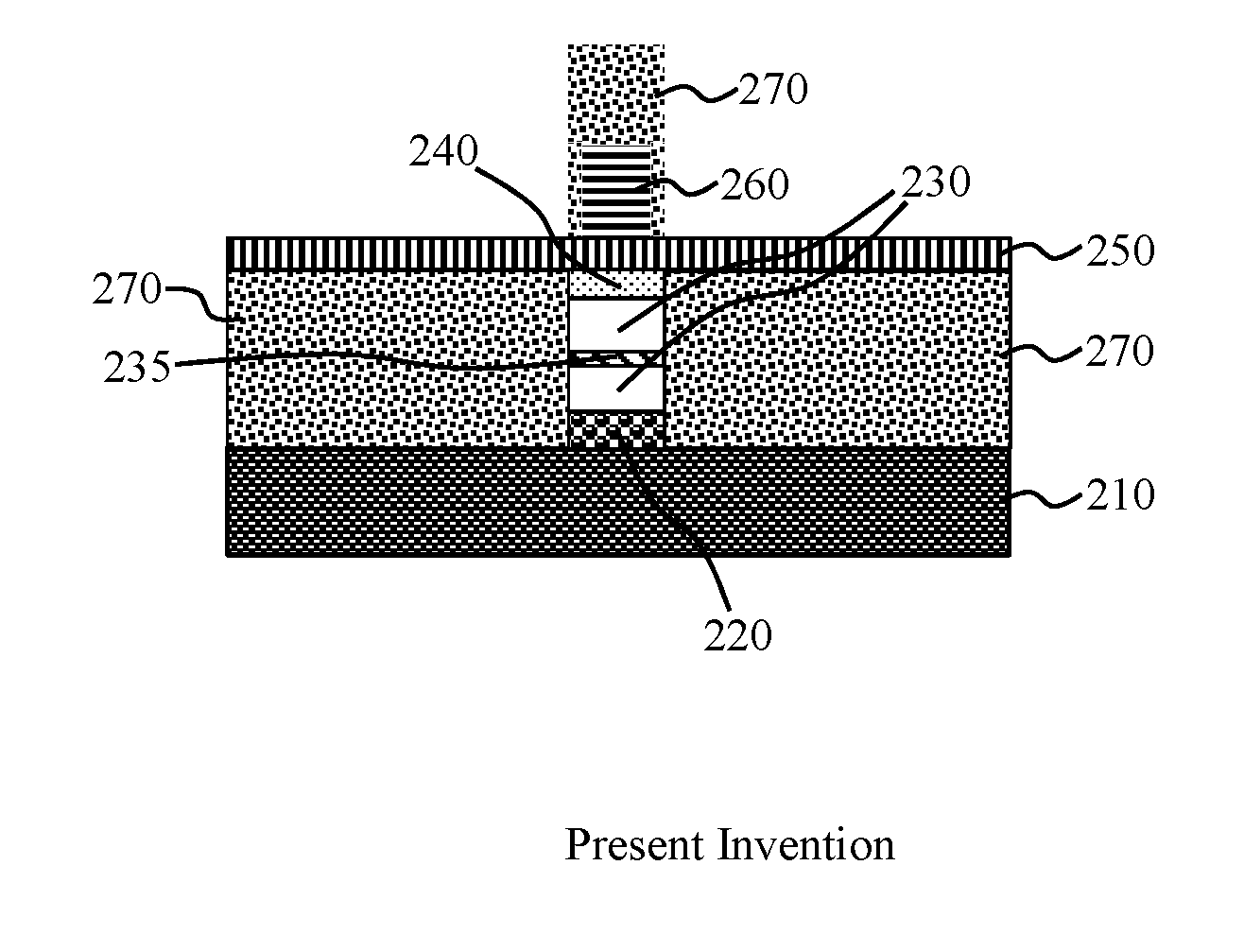
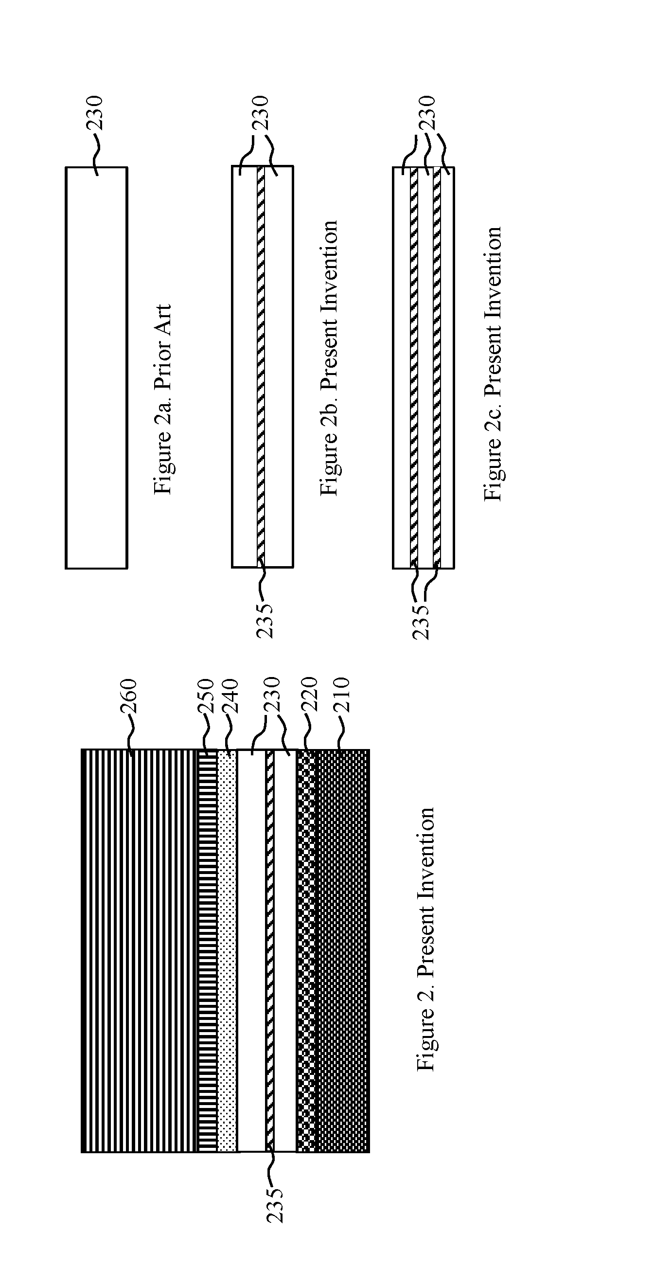
[0030]Similar to the earlier invention, our memory device still contains five core film stacks (FIG. 2): an ion implantation stopping layer (IISL) at the bottom (210), two oxygen getter layers (OGLs) (220&240) sandwich the middle magnetic layer magnetic memory layer (230), an ion-capping layer (250), and an ion-mask layer (260).

[0031]To better capture the oxygen ions implanted in the memory region, thus forming a uniformly distributed metal oxide dielectric (230 in FIG. 2) in the photolithography exposed area outside the device, we add an ultrathin oxygen-getter layer (235 in FIG. 2) into the middle magnetic layer. Such an OGL is selected from Mg, Zr, Y, Th, Ti, Al, Ba, with Mg as a preferred material due to its close MgO crystalline lattice match with the memory material. The thickness of such oxygen-getter layer (OGL) must be thin enough (230).

[0032]The IISL (210) typically contains a heavy metal with large atomic number, selected from Hf, Ta, W, Re, Os, Ir, Pt, Au, with a thickne...


PUM


Abstract

A method to make magnetic random access memory (MRAM), in particular, perpendicular spin transfer torque MRAM or p-STT-MRAIVI is provided. Electrically isolated memory cell is formed by ion implantation instead of etching and dielectric refill. Oxygen ion implantation is used to convert the photolithography exposed areas into metal oxide dielectric matrix. An ultrathin single-layer or multiple-layer of oxygen-getter, selected from Mg, Zr, Y, Th, Ti, Al, Ba is inserted into the active magnetic memory layer in addition to putting a thicker such material above and below the memory layer to effectively capture the impinged oxygen ions. Oxygen is further confined within the core device layer by adding oxygen stopping layer below the bottom oxygen-getter. After a high temperature anneal, a uniformly distributed and electrically insulated metal oxide dielectric is formed across the middle device layer outside the photolithography protected device area, thus forming MRAM cell without any physical deformation and damage at the device boundary.

Description

RELATED APPLICATIONS[0001]This application is a divisional application due to a restriction requirement on Application No. 14 / 273,501. This application seeks priority to U.S. Utility Patent Application No. 14 / 273,501 filed on May 8, 2014 and U. S. Provisional Patent Application No. 61,825,102 filed on May 20, 2013; the entire contents of each of which are incorporated herein by reference.BACKGROUND OF THE INVENTION[0002]1. Field of the Invention[0003]This invention relates generally to spin-electronic devices, more particularly to a magnetic random access memory and a method to make the same using oxygen ion implantation.[0004]2. Description of the Related Art[0005]Magnetoresistive elements having magnetic tunnel junctions (also called MTJs) have been used as magnetic sensing elements for years. In recent years, magnetic random access memories (hereinafter referred to as MRAMs) using the magnetoresistive effect of MTJ have been drawing increasing attention as the next-generation sol...

Claims


Application Information

Patent Timeline
Patent Type & Authority Applications(United States)
IPC IPC(8): H01L43/12H01L43/10
CPCH01L43/10H01L43/12H10N50/01H01L29/82H10N50/85
Inventor GUO, YIMIN
Owner T3MEMORY
Why Eureka
Try Eureka