Fabrication method for a thin film semiconductor device, the thin film semiconductor device itself, liquid crystal display, and electronic device

Inactive Publication Date: 2000-01-25
INTELLECTUAL KEYSTONE TECH
View PDF31 Cites 435 Cited by
  • Summary
  • Abstract
  • Description
  • Claims
  • Application Information

AI Technical Summary

Problems solved by technology

Such amorphous silicon layers, however, have such problems as electrical characteristics far inferior to those of polysilicon layers and slow operating speed.
Since the high temperature process polysilicon TFTs use quartz substrates, however, there are problems with increasing display size and decreasing costs.
But, when using large substrates which are well-suited to mass production, there is a severe restriction in that the substrates must be kept below a maximum processing temperature of about 570.degree. C. in order to avoid deformation of the substrates.
As described below, however, there are several inherent problems with poly--Si TFTs fabricated by the existing technology in the low temperature process which act as impediments to the adoption of this technology into mass production.
1. The high processing temperature of 550.degree. C. prevents the use of low-priced glass leading to a steep rise in product prices.
Additionally, the degree of warp of the glass substrates as a result of their own weight increases as substrate size increases, and increases in liquid crystal display (LCD) sizes are not possible.
As a result, the crystallization of the film can vary from uniform to non-uniform from lot to lot and reliable production is not possible.
3. During the ion doping or subsequent low temperature activation at 300-350.degree. C. of the source and drain regions which are self-aligned with respect to the gate electrode, the problem of unsuccessful activation occasionally occurs.
Especially when producing TFTs with lightly doped drains (LDD), this problem is serious and is a cause of significant decreases in production yield.
4. Although only SiO.sub.2 formed by ECR-PECVD yields suitable transistor properties-in low temperature process poly--Si TFTs, it is difficult to increase the size of the ECR source in the ECR-PECVD equipment thereby making ECR-PECVD unsuitable for large LCD panels.
Furthermore, the throughput is extremely poor.
Consequently, EC

Method used


Image

  • Fabrication method for a thin film semiconductor device, the thin film semiconductor device itself, liquid crystal display, and electronic device
  • Fabrication method for a thin film semiconductor device, the thin film semiconductor device itself, liquid crystal display, and electronic device
  • Fabrication method for a thin film semiconductor device, the thin film semiconductor device itself, liquid crystal display, and electronic device

Examples


Example

EXAMPLE 1

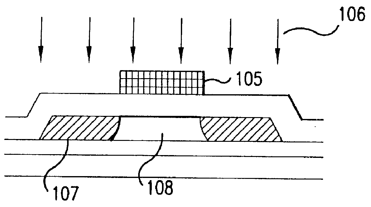
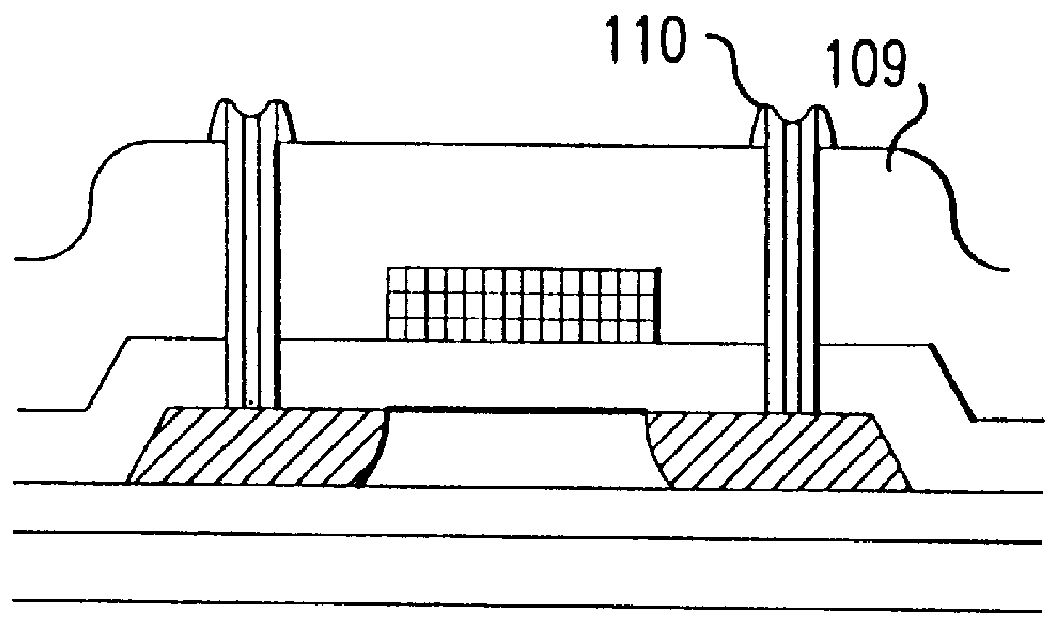
FIGS. 1(a) through (d) show cross-sectional views of the fabrication process for a thin film MIS field effect transistor.

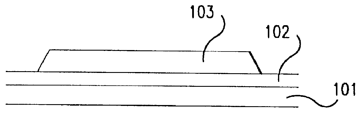
In Example 1, a 235 mm.times.235 mm sheet of non-alkaline glass (OA-2, manufactured by Nippon Electric Glass Co., Ltd.) was used for substrate 101, though the type and size of the substrate are irrelevant for any substrate able to withstand the maximum processing temperature. First, silicon dioxide film (SiO.sub.2 film) 102, which serves as the underlevel protection layer, is formed on substrate 101 by means of atmospheric pressure chemical vapor deposition (APCVD), PECVD, sputtering or other means. In APCVD, the SiO.sub.2 layer can be deposited using monosilane (SiH.sub.4) and oxygen as source gases at a substrate temperature of between about 250.degree. C. and 450.degree. C. In the PECVD and sputtering methods, the substrate temperature can be anywhere from room temperature to 400.degree. C. In Example 1, a 2000 .ANG. SiO.sub.2 film was deposited at 300...

Example

EXAMPLE 2

Other examples of implementations of this invention will also be explained using FIGS. 1(a) through (d).

In Example 2, sheets of non-alkaline glass (OA-2 manufactured by Nippon Electric Glass Co., Ltd.) measuring 300 mm.times.300 mm and crystallized glass (TRC-5 manufactured by Ohara) measuring 300 mm.times.300 mm were used for substrate 101. The strain point of OA-2 is approximately 650.degree. C. TRC-5, on the other hand, is a crystallized glass, so the strain point cannot be defined. Since absolutely no substrate deformation or warpage can be detected up to a temperature of about 700.degree. C., however, the strain point of TRC-5 can, in practice, be said to be above about 700.degree. C. First, silicon oxide film 102, which becomes the underlevel protection layer, was deposited by PECVD onto substrate 101. The silicon oxide film was deposited under the same conditions that the gate insulator layer was deposited in Example 1. The thickness of the silicon oxide film was 300...

Example

EXAMPLE 3

After forming the poly--Si.sup.- layer using the method described in detail in Example 1, an SiO.sub.2 layer corresponding to the gate insulator layer described in detail in Example 1 was deposited without patterning this poly--Si layer, and impurity ions such as PH.sub.3 were implanted in the poly--Si layer by ion doping, details of which were explained in Example 1. The thicknesses of the poly--Si layer and SiO.sub.2 layer and the conditions under which they were deposited were exactly the same as they were in Example 1. Impurity ion implantation conditions were also the same as those described in Example 1 except that the implantation dose was 3.times.10.sup.13 cm.sup.-2. Example 3 corresponds to the formation of the LDD region in TFTs explained in Example 1. After phosphorous ions were implanted, thermal annealing was performed at 300.degree. C. in oxygen for one hour, again just as in Example 1. After that the insulator layer was stripped off and the sheet resistance o...


PUM


Abstract

In order to fabricate a high performance thin film semiconductor device using a low temperature process in which it is possible to use low price glass substrates, a thin film semiconductor device has been fabricated by forming a silicon film at less than 450 DEG C., and, after crystallization, keeping the maximum processing temperature at or below 350 DEG C. In applying the present invention to the fabrication of an active matrix liquid crystal display, it is possible to both easily and reliably fabricate a large, high-quality liquid crystal display. Additionally, in applying the present invention to the fabrication of other electronic circuits as well, it is possible to both easily and reliably fabricate high-quality electronic circuits.

Description

FIELD OF TECHNOLOGYThe present invention is related to the fabrication method for a thin film semiconductor device, the thin film semiconductor device itself, liquid crystal displays, and electronic devices applicable to active matrix liquid crystal displays and the like.BACKGROUND TECHNOLOGYIn recent years, along with increases in screen size and improvements in resolution, the driving methods for liquid crystal displays (LCDs) are moving from simple matrix methods to active matrix methods; and the displays are becoming capable of displaying large amounts of information. LCDs with more than several hundreds of thousands pixels are possible with active matrix methods which place a switching transistor at each pixel. Transparent insulating substrates such as fused quartz and glass which allow the fabrication of transparent displays are used as substrates for all types of LCDs. Although ordinarily semiconductor layers such as amorphous silicon or polycrystalline silicon are used as th...

Claims


Application Information

Patent Timeline
IPC IPC(8): H01L29/40H01L21/336H01L21/205H01L29/49H01L21/02H01L21/28H01L29/786H01L29/66G02F1/13G02F1/1362F16C29/00G02F1/136H01L21/20H01L21/324
CPCF16C29/00H01L21/28079H01L21/3105H01L29/4908H01L29/66757H01L29/78675H01L21/0237H01L21/02521H01L21/02532H01L21/02576H01L21/02579H01L21/0262H01L21/02661G02F1/13454G02F2202/104F16C2360/45H01L29/768
Inventor MIYASAKA, MITSUTOSHI
Owner INTELLECTUAL KEYSTONE TECH
Why Eureka
Try Eureka