Method for forming crystalline semiconductor layers, a method for fabricating thin film transistors, and method for fabricating solar cells and active matrix liquid crystal devices

a technology of crystalline semiconductors and thin films, applied in transistors, final product manufacturing, basic electric elements, etc., can solve the problems of difficult to achieve high-quality semiconductor layers, suffer from poor throughput, and subject to important limitations

Inactive Publication Date: 2000-05-23
SEIKO EPSON CORP
View PDF12 Cites 163 Cited by
  • Summary
  • Abstract
  • Description
  • Claims
  • Application Information

AI Technical Summary

Benefits of technology

As described, this invention enabled the uniform fabrication of extremely good CMOS thin film semiconductor devices having high mobility on large, conventional glass substrates. The uniformity of laser crystallization, whether within a substrate or from lot to lot, has been a very serious problem in the low temperature process of the prior art. This invention, however, greatly reduces the nonuniformity of both on currents and off currents. This marked improvement in uniformity speaks for the validity of the fundamental principles of the present invention (Section 1). Following such principles, this invention achieves marked improvement even with respect to lot-to-lot fluctuations. As described, this invention enables silicon and other semiconductor films to be crystallized extremely reliably by means of laser or other high energy optical irradiation. Therefore, LCDs employing thin film semiconductor devices of this invention exhibit uniform high picture quality across the entire screen. Moreover, the thin film semiconductor devices of this invention can also easily be used to form not only simple circuits such as shift registers and analog switches but also more complex circuits such as level shifters, digital to analog converter circuits and even clock generator circuits, gamma correction circuits, and timing controller circuits.
Using the solar cell obtained in Example 4 as an auxiliary power supply, the liquid crystal display obtained as explained was installed in the body of a full-color portable personal computer (notebook PC). Since the active matrix substrate was equipped with integrated 6-bit digital data drivers and since digital video signals from the computer were input directly to the liquid crystal display device, the circuit configuration was simplified, while power consumption was simultaneously reduced to an extremely low level. The high performance of the liquid crystal thin film semiconductor device gave this notebook PC an extremely attractive display screen and made it a good electronic device. In addition, because this is a reflective liquid crystal display device with high aperture ratio, a backlight was unnecessary. The absence of a backlight and the integration of a high conversion efficiency solar cell as an auxiliary power supply made it possible to decrease the size and weight of the batteries while simultaneously extending the length of time they can be used. Accordingly, an extremely small, light-weight electronic device with a beautiful display screen that has the potential for long-time use was fabricated.
As stated above, the method of fabricating crystalline semiconductor layers and the method of fabricating cells thin film semiconductor devices such as thin film transistors and solar cells using such crystalline semiconductor layers described by this invention enable the manufacture of high performance thin film semiconductor devices using a low temperature process in which inexpensive glass substrates can be used. Therefore, applying this invention to the manufacture of active matrix liquid crystal display devices permits large-size, high-quality liquid crystal display devices to be manufactured easily and reliably; and, when used in solar cells, high conversion efficiency solar cells can be fabricated. Moreover, when this invention is applied to the manufacture of other electronic circuits, high quality electronic circuits can also be manufactured easily and reliably.
Additionally, because of their low cost and high performance, the thin film semiconductor devices of this invention are perfectly suited as the active matrix substrate of an active matrix liquid crystal display device. They are optimum devices to use as integrated-driver active matrix substrates that demand particularly high performance.

Problems solved by technology

However, the formation of this kind of high quality semiconductor layer is generally difficult to achieve and, moreover, is subject to important limitations.
However, the first of the conventional technologies (solid phase crystallization) requires annealing over a long period of time--more than 10 hours--and thus suffers from extremely poor throughput.
Moreover, in this process thermal deformation of the substrate arising from prolonged heating of the entire substrate has become a major problem, meaning essentially that inexpensive, large glass substrates cannot be used.
The problem with the second of the conventional technologies (laser crystallization) is that crystallization does not progress if the laser irradiation energy is too low, while high energy will damage the semiconductor film.
Hence, satisfactory, high quality crystalline films cannot be produced under either of the irradiation conditions.
Moreover, extensive nonuniformity in crystallinity is known to occur with each laser irradiation.
The result is that even if these semiconductor films are applied in TFTs, for example, good transistor characteristics cannot be obtained.
Nevertheless, this process, too, has essentially the same problems as those of the first method.
That is, even if the annealing temperature were kept to about 450.degree. C., throughput would be poor because annealing would be required for at least several hours and, moreover, thermal distortion of the substrate could not be ignored.
Incomplete crystallization in which the degree of crystallinity is low is basically caused by a lack of sufficient energy and has a tendency to occur in methods such as VST-SPC.
The larger the incidence of amorphous components, the closer the electrical characteristics are to that of an amorphous material, making the product unsatisfactory as a crystalline semiconductor layer.
Moreover, as a result of scattering by out-of-position atoms, a decrease in characteristics such as mobility is unavoidable.
Crystalline layers created by VST-SPC and by melt crystallization employing laser or high energy optical irradiation do not make good films simply because they exhibit to a greater or lesser extent these three problems (incomplete crystallization, deviation from regular lattice points, and irregular grain boundaries).
atures. In addition, the reason that such a long time for crystallization in the solid phase is necessary is that the generation of crystal nuclei
aling step. As stated above, the problem of internal grain defects and deviation from the regular lattice points (high internal stress) is caused in part by the rapid solidificat
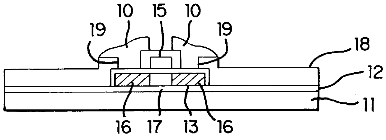
If the thickness of the insulating layer is too thick, cracks can appear as a result of stress in the insulating layer.
Crystallization over the entire thickness of a 400 nm or thicker semiconductor layer (especially silicon) even using a relatively long wavelength laser such as HeNe (632.8 nm) is difficult.
On the other hand, such light is naturally essentially unabsorbed by transparent substrates.
During electrode formation, these undesirable structures can be causes of poor contact between the electrode and underlying layers in the device leading to so-called "contact failure."
If the .beta. value is too large, however, cheap conventional glass substrates will deform from thermal stresses or crack, and cannot be used.

Method used


Image

  • Method for forming crystalline semiconductor layers, a method for fabricating thin film transistors, and method for fabricating solar cells and active matrix liquid crystal devices
  • Method for forming crystalline semiconductor layers, a method for fabricating thin film transistors, and method for fabricating solar cells and active matrix liquid crystal devices
  • Method for forming crystalline semiconductor layers, a method for fabricating thin film transistors, and method for fabricating solar cells and active matrix liquid crystal devices

Examples


example 1

The explanation for this example will refer to FIG. 6. First, after an underlevel protection layer is formed on the surface of conventional glass substrate 20 (the underlevel protection layer is not shown in FIG. 6 for simplicity), the substrate-side first electrode (indium tin oxide (ITO) in this example) 21 is formed on top of this underlevel protection layer. This is formed by using photolithography after the deposition of a conducting film by a method such as normal sputtering. Because the present example supposes a solar cell structure in which the light is incident on the semiconductor layer from the substrate side (the bottom side in FIG. 6), transparent glass is used for the substrate and the substrate-side first electrode is also formed from a transparent conducting film. For the opposite structure in which the light incident on the semiconductor layer comes from the element side (the top side in FIG. 6), however, if the element-side second electrode is a transparent conduc...

example 2

In Example 1 the formation of the first conductive semiconductor layer and the second conductive semiconductor layer was carried out by impurity diffusion into the intrinsic semiconductor layer, but in this example, impurity containing semiconductor layers are formed by a method such as CVD and solar cells are fabricated (refer to FIG. 7).

As in Example 1, after an underlevel protection layer is formed on the surface of conventional glass substrate 30 (in FIG. 7 as well, the underlevel protection layer is not shown for the sake of simplicity), substrate-side first electrode (indium tin oxide (ITO) in this example) 31 is formed on top of this underlevel protection layer (FIG. 7(a)). Next, first conductive semiconductor layer 32, essentially intrinsic semiconductor layer 33, and second conductive semiconductor layer 34 are formed in a layered structure on the surface of the substrate-side first electrode by a method such as CVD (FIG. 7(b)). In this example, p-type silicon film 32 is de...

example 3

While Example 1 showed an example of a solar cell structure in which the light was incident upon the semiconductor layer from the substrate side, this example shows one example of a structure in which the light is incident from the element side (the top side in FIG. 8) in contrast to Example 1 (refer to FIG. 8).

First, after forming an underlevel protection layer as necessary on the surface of substrate 40, which is inexpensive and has relatively good flatness such as might be found with glass, substrate-side first electrode 41 is formed from a material such as aluminum or platinum. As the material for the substrate-side first electrode, a conductive material such as a metal with high light reflectivity and high electrical conductivity is desirable. There are no special limitations on the substrate as long as it is stable with respect to thermal processing steps and chemicals in the fabrication of solar cells. Substrate-side first electrode 41 is formed by photolithography following ...


PUM

PropertyMeasurementUnit
thermal resistanceaaaaaaaaaa
temperatureaaaaaaaaaa

Abstract

PCT No. PCT / JP96 / 01775 Sec. 371 Date Jan. 31, 1997 Sec. 102(e) Date Jan. 31, 1997 PCT Filed Jun. 26, 1996 PCT Pub. No. WO97 / 01863 PCT Pub. Date Jan. 16, 1997A crystalline semiconductor layer can be formed by forming a semiconductor film on an inexpensive conventional substrate. Next, perform a first annealing process in which nearly the entire surface of the semiconductor film is exposed to laser irradiation or other forms of irradiation, and then perform a second annealing process consisting of rapid thermal annealing. This enables the formation of a high quality crystalline semiconductor film with high throughput but without subjecting the substrate to undue thermal stress. When this invention is applied to thin film transistors, good transistors having high performance are easily fabricated. When this invention is applied to solar cells, energy conversion efficiency is increased.

Description

1. Field of the InventionThis invention concerns a method for forming crystalline semiconductor layers and a method for fabricating thin film transistors, active matrix liquid crystal devices and solar cells that employ these crystalline semiconductor layers.2. Description of the Related ArtPolycrystalline silicon and other semiconductor films are used widely in thin film transistors ("TFT" in the specifications of this application) and solar cells. The performance of these semiconductor devices is strongly dependent on the quality of the semiconductor layer, which wholly constitutes the active portion of the semiconductor device. Needless to say, if a high-quality semiconductor layer can be created, a semiconductor device with correspondingly high performance can be produced. For example, in a polycrystalline silicon thin film transistor (poly-Si TFT) used in such products as liquid crystal display devices, the higher the quality of the polycrystalline silicon (poly-Si) layer, the ...

Claims


Application Information

Patent Timeline
Patent Type & Authority Patents(United States)
IPC IPC(8): H01L21/02H01L21/20H01L31/18
CPCH01L21/2022H01L31/1864Y02E10/50Y02P70/50H01L21/02683H01L21/02488H01L21/02422H01L21/02463H01L21/0242H01L21/0262H01L21/02466H01L21/02425H01L21/02686H01L21/0245H01L21/02378H01L21/02381H01L21/02691H01L21/02477H01L21/02447H01L21/20H01L29/786H01L31/0392H01L21/02675H01L21/02667
Inventor MIYASAKA, MITSUTOSHI
Owner SEIKO EPSON CORP
Why Eureka
Try Eureka