
Amorphous dielectric capacitors on silicon

a dielectric capacitor and silicon technology, applied in the field of high-capacitance capacitors, can solve the problems of high device leakage, low dielectric constant materials, and inability to meet the needs of high-capacitance capacitors,

Inactive Publication Date: 2001-07-03
GLOBALFOUNDRIES INC
View PDF12 Cites 49 Cited by
  • Summary
  • Abstract
  • Description
  • Claims
  • Application Information

AI Technical Summary

Benefits of technology

A further object of the present invention is to provide a thin film dielectric material which exhibits good conformity to the electrode material to which it is applied as well as a low leakage current that is on the order of 1 A / cm.sup.2 or less, preferably 1.times.10.sup.-4 A / cm.sup.2 or less.
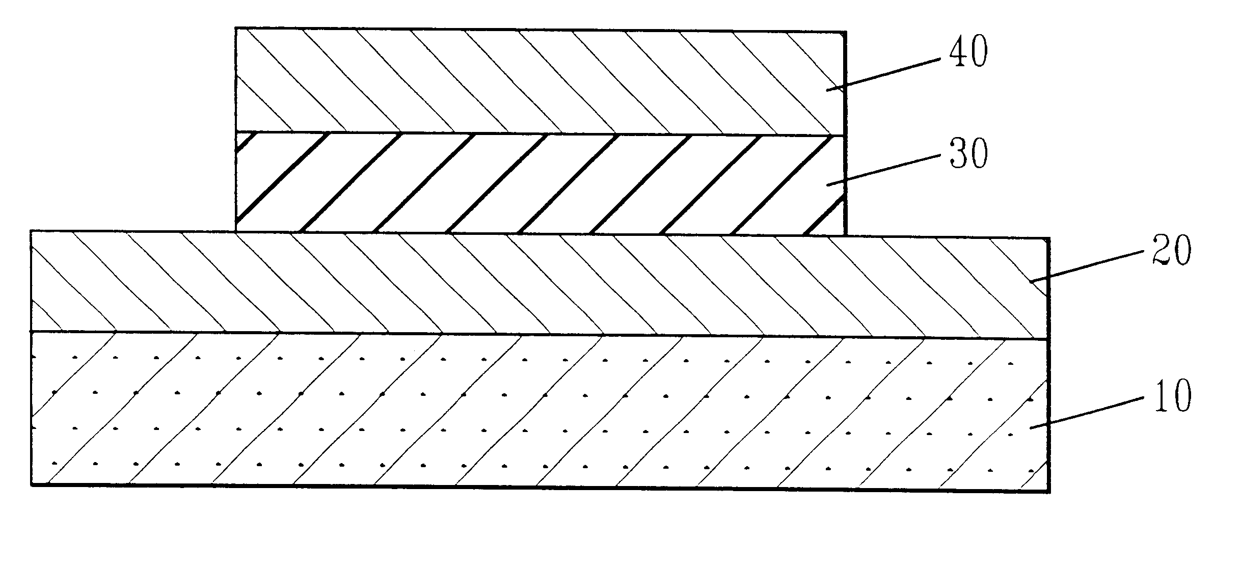
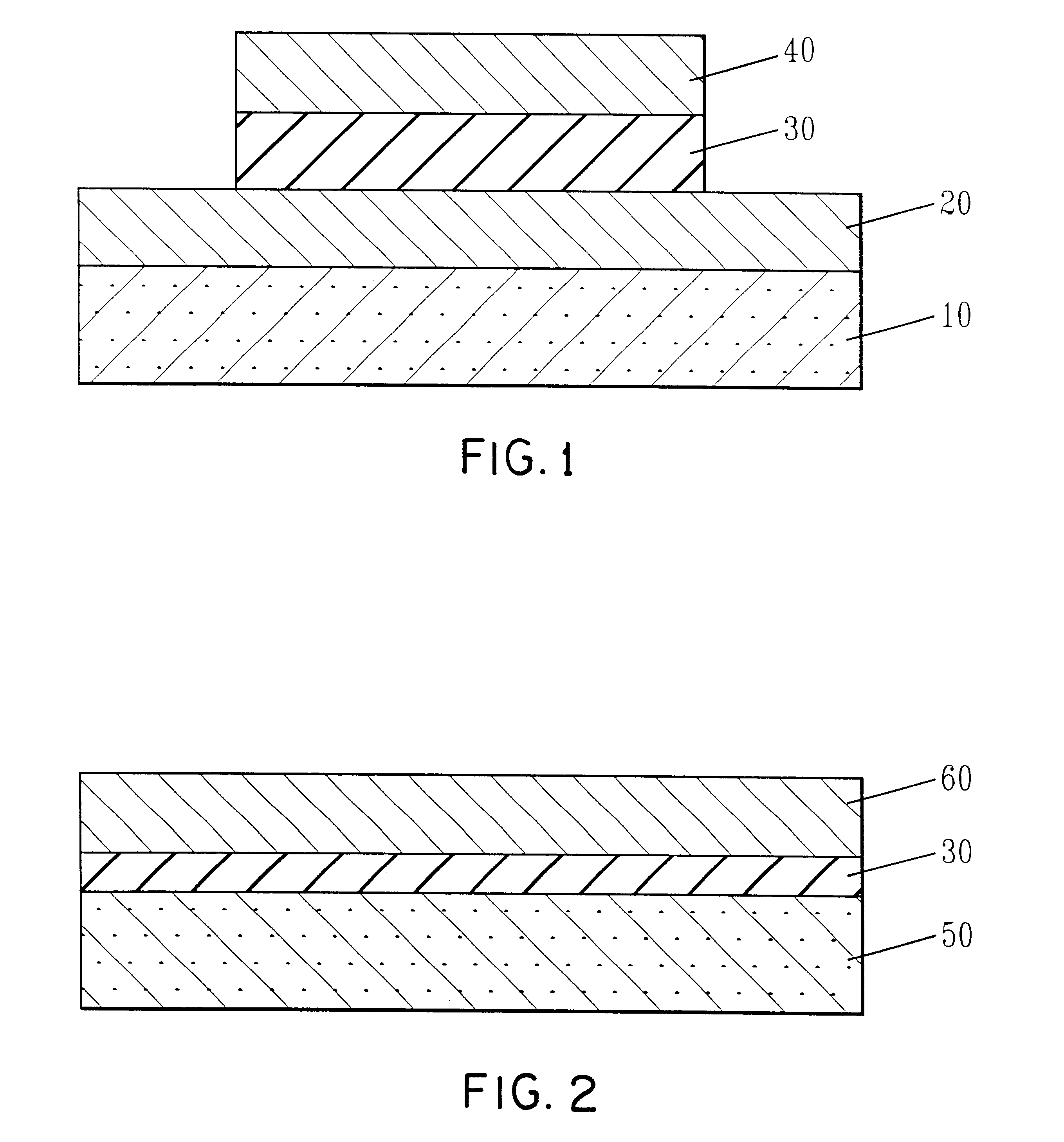
These and other objects and advantages are achieved in the present invention by utilizing an amorphous (or low temperature) phase material as a thin film dielectric material. Specifically, one embodiment of the present invention relates to high-capacitance capacitors (on the order of 1 nF / mm.sup.2 or above) formed using thin films of materials which are in the amorphous (or low temperature) phase. Such dielectric materials can be formed directly on top of silicon minimizing the formation of any interfacial layers or grain boundaries which can lead to device degradation.
In the latter stages of CMOS processing and in applications such as BEOL structures and organic FETs, ambient temperatures must be kept low, less than 500.degree. C., thus the novel capacitors and transistors of the present invention use a low temperature deposition and annealing process to stay at or below this temperature. These low temperature processes ensure formation of a dielectric material which is in the amorphous (or low temperature) phase. For example, it has been determined that the low temperature (or amorphous) phase of barium strontium titanate has a dielectric constant of up to about 25 which value is significantly higher than that of the typical dielectrics used in circuit applications. Other perovskite-type oxides such as lead lanthanum titanate can have even greater dielectric constants in their amorphous phase. Capacitors and transistors formed utilizing these particular types of low temperature dielectrics also exhibit low leakage and good conformability.
(c) annealing the amorphous dielectric material at a temperature which is effective in improving the quality as well as the dielectric constant of the amorphous dielectric material; and
(b) annealing the amorphous high dielectric constant material at a temperature which is effective in improving the quality as well as the dielectric constant of the amorphous dielectric material; and

Problems solved by technology

The use of thin, low dielectric constant materials in today's circuits is undesirable since such materials lead to leaky circuits.
At such high temperatures, if deposited directly on silicon, interfacial layers form which may degrade device performance.
In addition, grain boundary leakage paths and lowered barrier heights may result which could lead to high device leakage.
The only critical limitation is that the deposition and annealing temperatures be below the crystalline temperature of the perovskite-type oxide.

Method used


Image

  • Amorphous dielectric capacitors on silicon
  • Amorphous dielectric capacitors on silicon

Examples


Embodiment Construction

An example of the fabrication of amorphous or low temperature thin film dielectric material of the present invention by chemical solution deposition is given below. Under nitrogen with stirring, 0.035 mole barium methoxyethoxide, 0.015 mole strontium methoxyethoxide, and 0.050 mole titanium methoxyethoxide were dissolved together in 2-methoxyethanol. The solution was stirred overnight at room temperature, filtered and diluted to the mark in a 250 ml volumetric flask. A spin solution was prepared by diluting 1 part Ba.sub.0.7 Sr.sub.0.3 Ti methoxyethoxide stock solution with one part isopropanol.

The spin solution was loaded into a syringe and a 0.45 .mu.m and 0.1 .mu.m Whatman syringe filters were attached. The solution was syringed onto a heavily-doped p-type boron doped silicon substrate until the substrate was completely wetted. The substrate was then spun for 30 sec at 2500 rpm. The coated substrate was baked in an oxygen atmosphere in a furnace at 400.degree. C. for 5-10 min. Th...


PUM

PropertyMeasurementUnit
dielectric constantaaaaaaaaaa
temperaturesaaaaaaaaaa
thicknessaaaaaaaaaa

Abstract

High-capacity capacitors and gate insulators exhibiting moderately high dielectric constants with surprisingly low leakage using amorphous or low temperature films of perovskite type oxides including a titanate system material such as barium titanate, strontium titanate, barium strontium titanate (BST), lead titanate, lead zirconate titanate, lead lanthanum zirconate titanate, barium lanthanum titanate, a niobate, aluminate or tantalate system material such as lead magnesium niobate, lithium niobate lithium tantalate, potassium niobate and potassium tantalum niobate, a tungsten-bronze system material such as barium strontium niobate, lead barium niobate, barium titanium niobate, and Bi-layered perovskite system material such as strontium bismuth tantalate, bismuth titanate deposited directly on a silicon surface at temperatures about 450° C. or less.

Description

DESCRIPTION1. Field of the InventionThe present invention relates to high-capacitance capacitors, and more particular to an amorphous (or low temperature) phase of a high dielectric constant thin film material which can be employed as a dielectric in capacitors formed directly on silicon. Such structures will be useful as capacitors in dynamic random access memory (DRAM) applications, gate dielectrics in transistors and as decoupling capacitors. The present invention also relates to a gate dielectric material, and more particular to an amorphous (or low temperature) phase high dielectric constant thin film material which can be employed as a gate dielectric in a transistor.2. Background of the InventionDielectric materials in high density circuits appear as capacitors in dynamic random access memory (DRAM) applications, gate dielectrics in transistors and as decoupling capacitors. The dielectric materials in these structures are typically silicon dioxide (SiO.sub.2), silicon nitride...

Claims


Application Information

Patent Timeline
Patent Type & Authority Patents(United States)
IPC IPC(8): H01L21/02H10B12/00
CPCH01L28/55H10B12/00
Inventor DUNCOMBE, PETER RICHARDLAIBOWITZ, ROBERT BENJAMINNEUMAYER, DEBORAH ANNSHAW, THOMAS MCCARROLL
Owner GLOBALFOUNDRIES INC
Learn More