Heatsink and fabrication method thereof

a technology of heatsink and fabrication method, which is applied in the field of heatsink and a fabrication method thereof, can solve the problems of preventing proper performance, increasing the cost of the heatsink, and generating a large amount of heat during operation of high-power semiconductor devices, so as to improve the number of contact points between the substrate and the thin diamond film layer, improve the number of diamond film layer adherence, and improve the effect of the nucleus generation density

Inactive Publication Date:
View PDF11 Cites 30 Cited by
  • Summary
  • Abstract
  • Description
  • Claims
  • Application Information

AI Technical Summary

Benefits of technology

multidot.K in order to exhibit the advantage of the present invention.
W particles are exposed at the surface of the substrate. The surface roughness R.sub.Z of the W particle is preferably at least 0.05 .mu.m. The diamond nucleus is easily generated from the convex portion of the W particle. By setting the surface roughness R.sub.Z of the W particle as above, the nucleus generation density of diamond is improved. Therefore, the number of contact points between the substrate and the thin diamond film layer is increased. Thus, adherence between the thin diamond film layer and the substrate can further be improved.
If the surface roughness R.sub.Z of the W particle is less than 0.05 .mu.m, the nucleus generation density is reduced since the convex portion in the W particle is reduced. This means that the adherence between the thin diamond film layer and the substrate is degraded so that the thin diamond film layer easily peels off the substrate.
Preferably, an intermediate layer in which the Cu content is approximately 0% by weight is formed betw

Problems solved by technology

The aforementioned high power semiconductor devices generate a great amount of heat during operation.
Since natural diamond is precious and artificial diamond is costly, the cost of the heatsink will increase if the amount of diamond therein becomes greater.
Therefore, a heatsink formed entirely of diamond is used with respect to a semiconductor element of high heat generation such as a high power laser only in the application where heat radiation is so insufficient that it prevents exhibition of proper performance when a substitute is used or in the application such as during the stage of research where the cost is not yet estimated.
It can be said that a heatsink of higher thermal conductivity becomes more expensive.
However, the level of the heat radiation characteristic that is currently required has become so high that even BeO is even not sufficient.
However, it is difficult to process BeO per se.
Furthermore, BeO is toxic.
However, there was problem that it is difficult to grow a thin diamond film on a subs

Method used


Image

  • Heatsink and fabrication method thereof
  • Heatsink and fabrication method thereof
  • Heatsink and fabrication method thereof

Examples


example 2

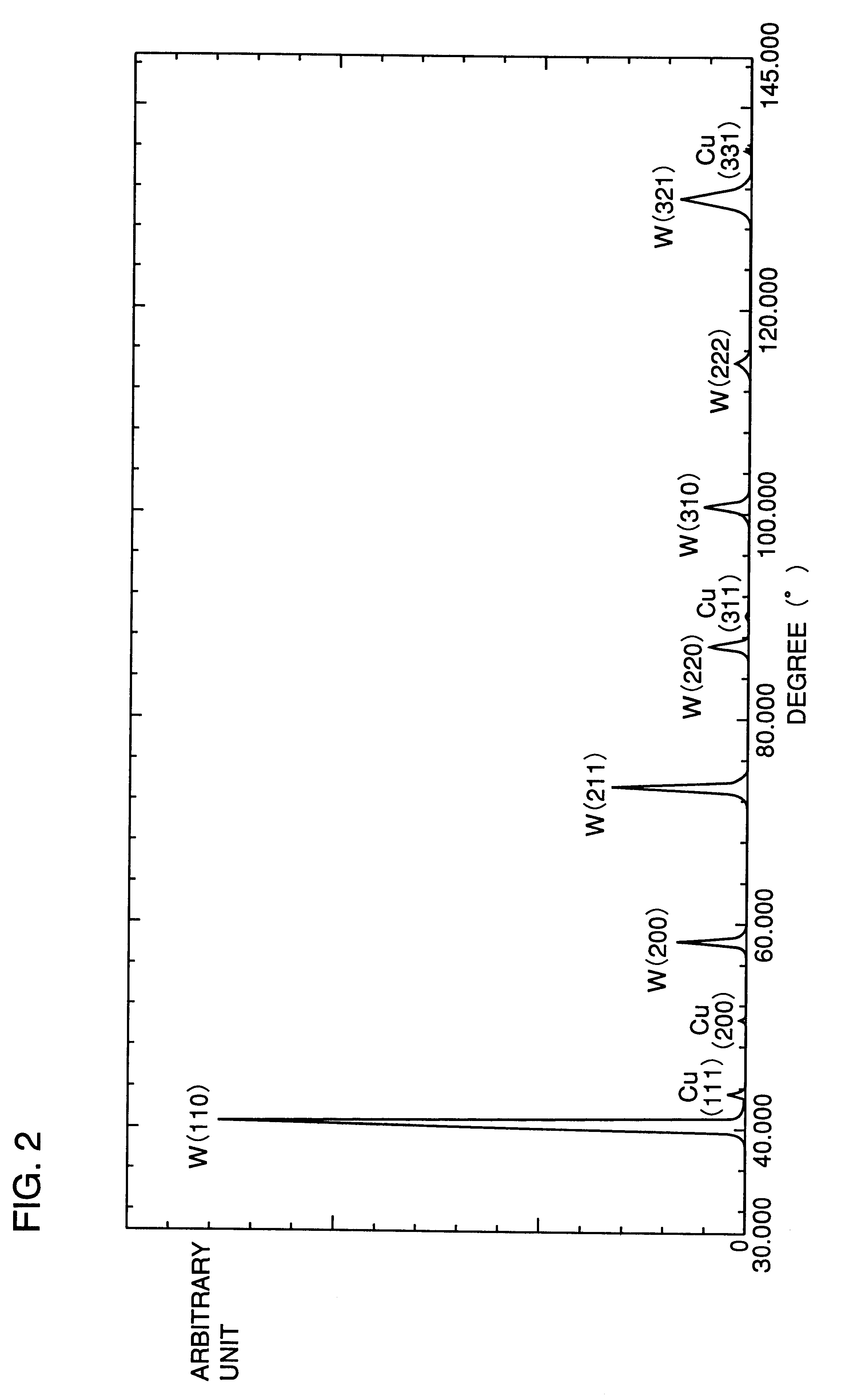
A substrate 26 was prepared formed of a Cu--W sintered compact with the Cu content of 15% by weight and 13.5 mm.times.13.5 mm.times.0.635 mm in size (lengthwise.times.breadthwise.times.thickness) as shown in FIG. 17. The surface of substrate 26 was roughened so that the surface roughness R.sub.Z of the substrate was 1 .mu.m. Here, R.sub.Z refers to the ten point height of irregularities defined by JIS (Japanese Industrial Standards).

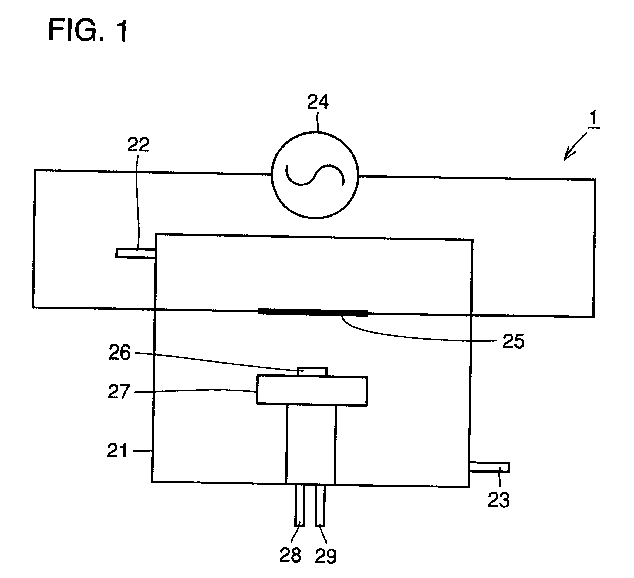
On the surface subjected to the above roughening process, SiC 32 as shown in FIG. 17 was deposited to 3 .mu.m in thickness as an intermediate layer not including Cu. The surface of the intermediate layer was scratched with diamond abrasive grains. Then, substrate 26 was mounted on substrate holder 27 in hot filament CVD apparatus 1 of FIG. 1. The temperature of tungsten filament 25 was set to approximately 2100.degree. C. Mixture gas of methane and hydrogen with the methane concentration of 1 mole % was introduced into reactor 21 through gas inlet 22. Th...

example 3

FIG. 7 is a schematic diagram showing a microwave plasma CVD apparatus for diamond vapor synthesis employed in the present invention. Microwave plasma CVD apparatus 100 includes a substrate holder 101, a microwave power source 104, a tuner 105, a wave guide 106, a reactor 107, an outlet 108, an inlet 109, and a plunger 110.

Substrate holder 101 for supporting a substrate is provided within reactor 107. Reactor 107 includes inlet 109 from which material gas is introduced and outlet 108 from which the material gas or gas generated by the reaction is output. Outlet 108 is connected to a vacuum pump. Microwave power source 104, an isolator (not shown) and a tuner 105 form the microwave generation unit. Reactor 107 is formed of a quartz tube.

The microwave generated from the microwave generation unit is directed towards plunger 110 via wave guide 106. Since reactor 107 is provided in the passage of wave guide 106, plasma is generated within reactor 107 as indicated by the circled dotted li...

example 4

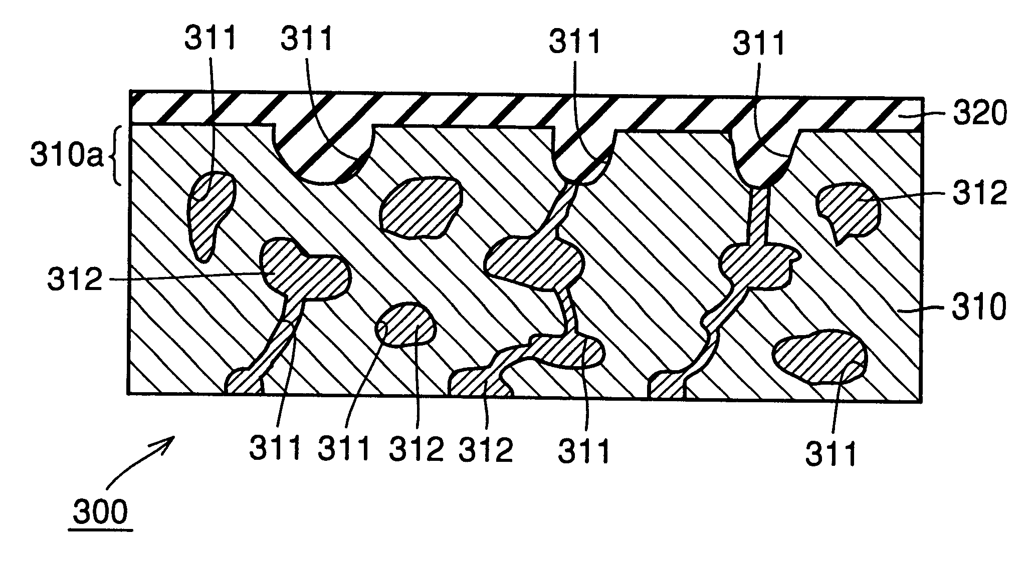
A porous body of 10 mm.times.10 mm.times.0.3 mm (lengthwise.times.breadthwise.times.thickness) in size was prepared, formed of a W sintered compact with the porosity of 27.5% by volume. Cu was permeated into the hole of the porous body. Accordingly, the entire Cu content of the substrate was set to 10% by weight, and the Cu content at the region of 10 .mu.m in depth from the surface where a thin diamond film layer is to be formed was set to 3% by weight.

The surface of the substrate was subjected to a scratching process using diamond abrasive grains. Substrate 102 was mounted on substrate holder 101 in microwave plasma CVD apparatus 100 shown in FIG. 7. The temperature of substrate 102 was set to 850.degree. C. Mixture gas of methane and hydrogen with the methane concentration of 3.5 mole % was introduced into reactor 107 through inlet 109. The pressure in reactor 107 was set to 140 Torr. A thin diamond film layer was grown on substrate 102 over 20 hours. The thin diamond film layer ...


PUM

PropertyMeasurementUnit
Fractionaaaaaaaaaa
Percent by massaaaaaaaaaa

Abstract

A thin diamond film layer is formed on a substrate with good adherence. A heatsink includes a substrate of a sintered compact including Cu and W, and a thin diamond film layer formed on the surface of the substrate. The Cu content in the substrate is at least 5% by weight. In an X-ray diffraction chart obtained by irradiating the thin diamond film layer with an X-ray, the diffraction peak intensity of the (110) plane of W is at least 100 times the diffraction peak intensity of the (200) plane of Cu.

Description

1. Field of the InventionThe present invention relates to a heatsink and a fabrication method thereof. Particularly, the present invention relates to a heatsink on which is mounted a semiconductor element of relatively great heat generation such as a laser diode, a CPU (central processing unit), a MPU (microprocessor unit), a high frequency amplifier device, and the like, having a multilayer structure of a diamond layer and a metal layer, and a method of fabricating such a heatsink.2. Description of the Background ArtThe aforementioned high power semiconductor devices generate a great amount of heat during operation. The heat generated by these semiconductor elements has become greater in accordance with improvement in the output and the operating frequency. The need of compact and light-weight electronic equipment is great in the industry while the packaging density of the semiconductor element is continuously increasing. The increase in the heat generation and packaging density of...

Claims


Application Information

Patent Timeline
IPC IPC(8): H01L21/02H01L21/48H01L23/12H01L23/48H01L23/14H01L23/495H01L23/34H01L23/373
CPCH01L21/4871H01L23/142H01L23/3732H01L23/3736H01L23/49562H01L2924/1423Y10T428/24975H01L2924/0002Y10T428/26Y10T428/24942Y10T428/30H01L2924/00Y10T428/249961Y10T428/249967Y10T428/249988Y10T428/24999Y10T428/31678
Inventor SAITO, HIROHISAYAMAMOTO, YOSHIYUKIMEGURO, KIICHIIMAI, TAKAHIRO
Why Eureka
Try Eureka