Disclosed herein is a non-oxidizing spacer densification method for producing semiconductor devices including, but not limited to,
MOSFET devices such as fully integrated complementary metal-
oxide semiconductor (“
CMOS”) devices having non-
volatile memory. Advantageously, the disclosed method may be implemented during semiconductor fabrication to provide low cost and robust processes for polycide formation with little or substantially no adhesion loss experienced during spacer oxide densification steps. The disclosed method also makes possible good polycide adhesion characteristics with reduced
process complexity over conventional methods by eliminating the need for additional process steps such as
metal silicide encapsulation or polysilicon surface treatments. The disclosed method further simplifies the spacer oxide densification step and process sequence since no
thermal oxide is grown over the non-
volatile memory stack structure, non-
memory control gate stack structure and source / drain regions during spacer densification, eliminating the need to manage
thermal oxide growth during this step. Further, the disclosed non-oxidizing method may be used to achieve MOSFET spacer oxide densification while at the same time minimizing or substantially preventing off-site oxide growth loss due to oxidation of exposed
silicon surfaces during the densification step.
By employing non-oxidizing species in a MOSFET spacer densification step, the disclosed method surprisingly eliminates the need for the added complexity of a metal
silicide top encapsulation layer and the need for controlled oxidation conditions during spacer densification employed in the practice of conventional MOSFET fabrication methods without detrimental effects on the performance of MOSFET transistors. This method of fabrication is contrary to accepted MOSFET spacer densification methodology that employs oxidizing species to grow a
thin layer of
silicon dioxide in the source and drain areas during spacer densification before, for example, deposition of polysilicon metal
dielectric layers.
Thus, in one embodiment, the disclosed method may be practiced to minimize or substantially eliminate undesirable growth of oxidation products (e.g., WxSiyO2 on
tungsten-based polycide layers) that are believed to result in polycide adhesion loss, and implementation of MOSFET spacer densification in a non-oxidizing environment eliminates the need for encapsulation methods to prevent polycide adhesion loss. Further, the disclosed method makes the spacer etch step substantially completely tolerant or independent of micro-loading effects, i.e., differences in amount of anti-
reflective layer that is removed from the top of the polycide layer during spacer etch steps. In this regard, the disclosed method may be successfully practiced under conditions
ranging from substantially
no removal of anti-
reflective layer during spacer oxide etch to almost complete removal of anti-
reflective layer during spacer oxide etch (e.g., only a few mono-layers of anti-reflective layer remaining). This characteristic advantageously reduces expense and complexity of the spacer oxide etch step.
Advantageously, the disclosed method may be further implemented in a low cost manner to fabricate high yield and high reliability polycide layers in an existing MOSFET fabrication unit. In this regard, the disclosed method may be implemented in a manner that reduces necessary
capital investment by using existing
physical vapor deposition (“PVD”) equipment for the
sputter deposition of metal silicide, e.g., by addition of a sputter chamber to existing PVD equipment. Additional
cost savings may be realized by using
rapid thermal processing (“RTP”) methodology, e.g., low DT (e.g. time at temperature), rather than slow controlled furnace tube oxidizing anneal methodologies that are employed in conventional spacer densification methods. Further cost advantages may be realized using the disclosed method by employing
plasma enhanced
chemical vapor deposition (“PECVD”) for anti-reflective layer (“ARL”) deposition rather than using the costlier spin-on deposition of ARL.
In another respect, disclosed herein is a relatively low cost and
high yielding method for the integration of
tungsten polycide deposition into an existing
CMOS fabrication facility. In one embodiment, the method may combine the
physical vapor deposition (“PVD”) or
sputter deposition of a tungsten polycide layer,
plasma enhanced
chemical vapor deposition (“PECVD”) of a
silicon oxynitride anti-reflective layer (“ARL”), and rapid thermal processor spacer densification in the presence of a non-oxidizing species (e.g.,
nitrogen) to produce a non-encapsulated polycide layer having good adhesion characteristics. In this embodiment, RTP in a non-oxidizing
nitrogen environment advantageously may be employed to achieve spacer densification without the need for encapsulation methods to prevent polycide adhesion loss.
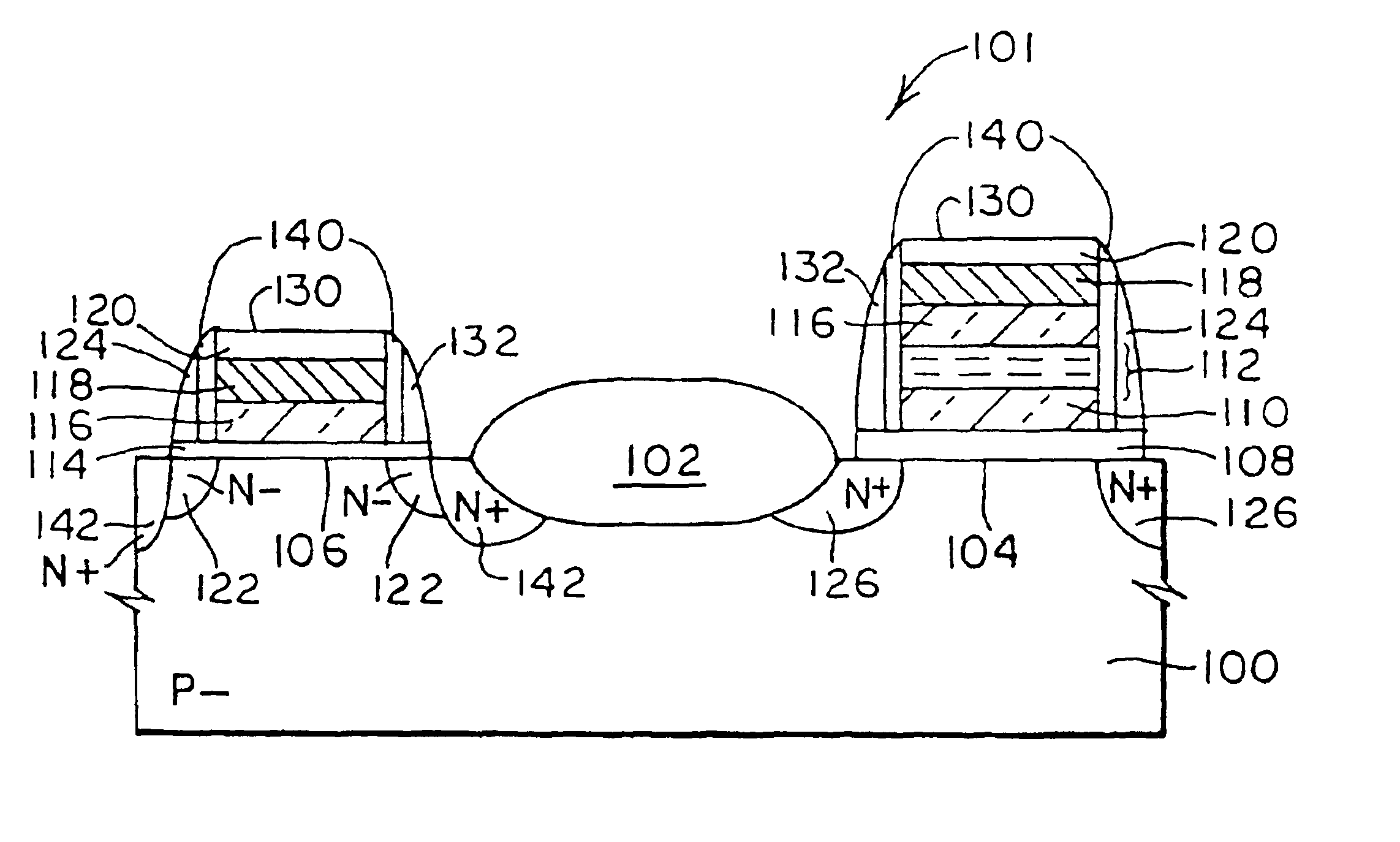
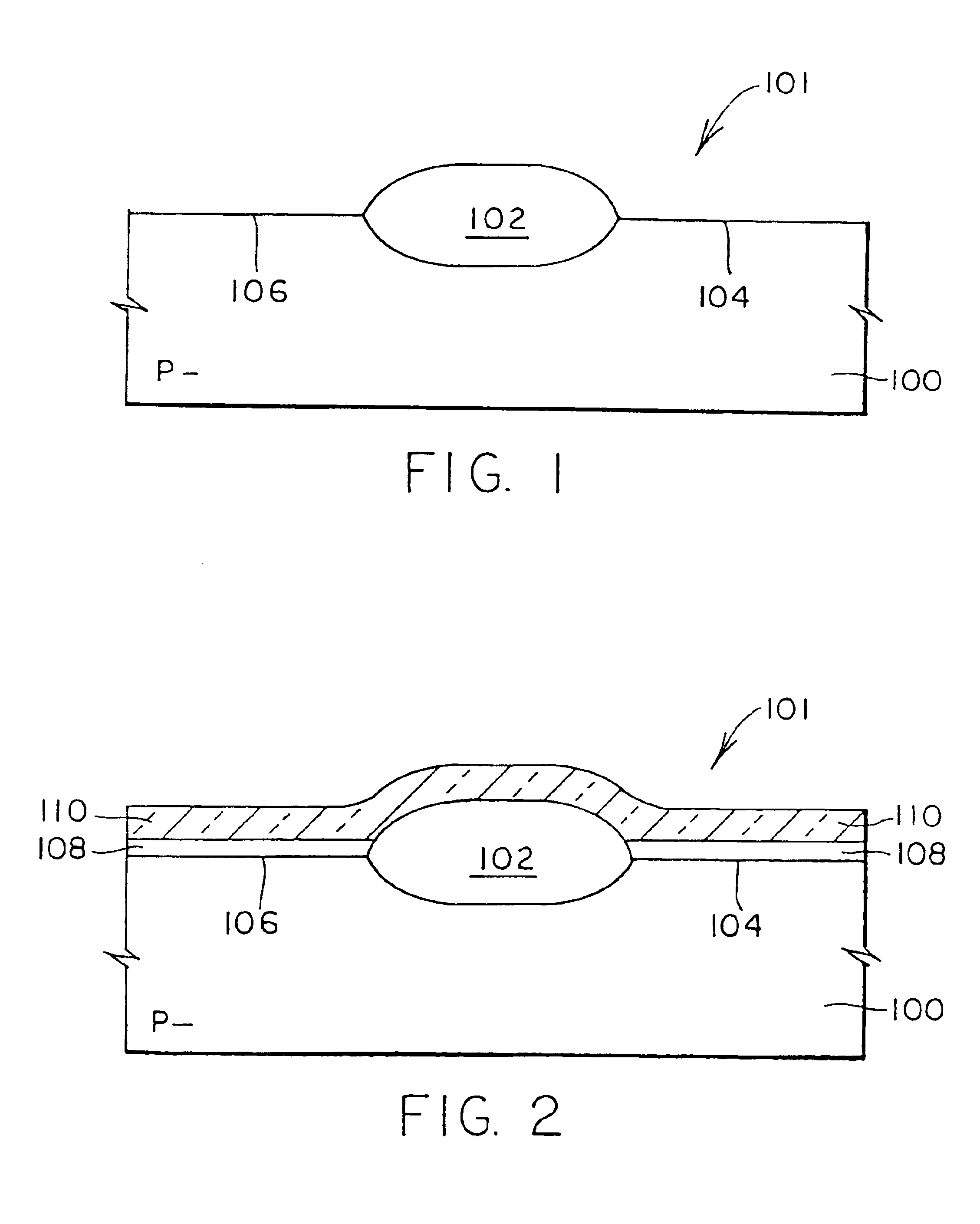
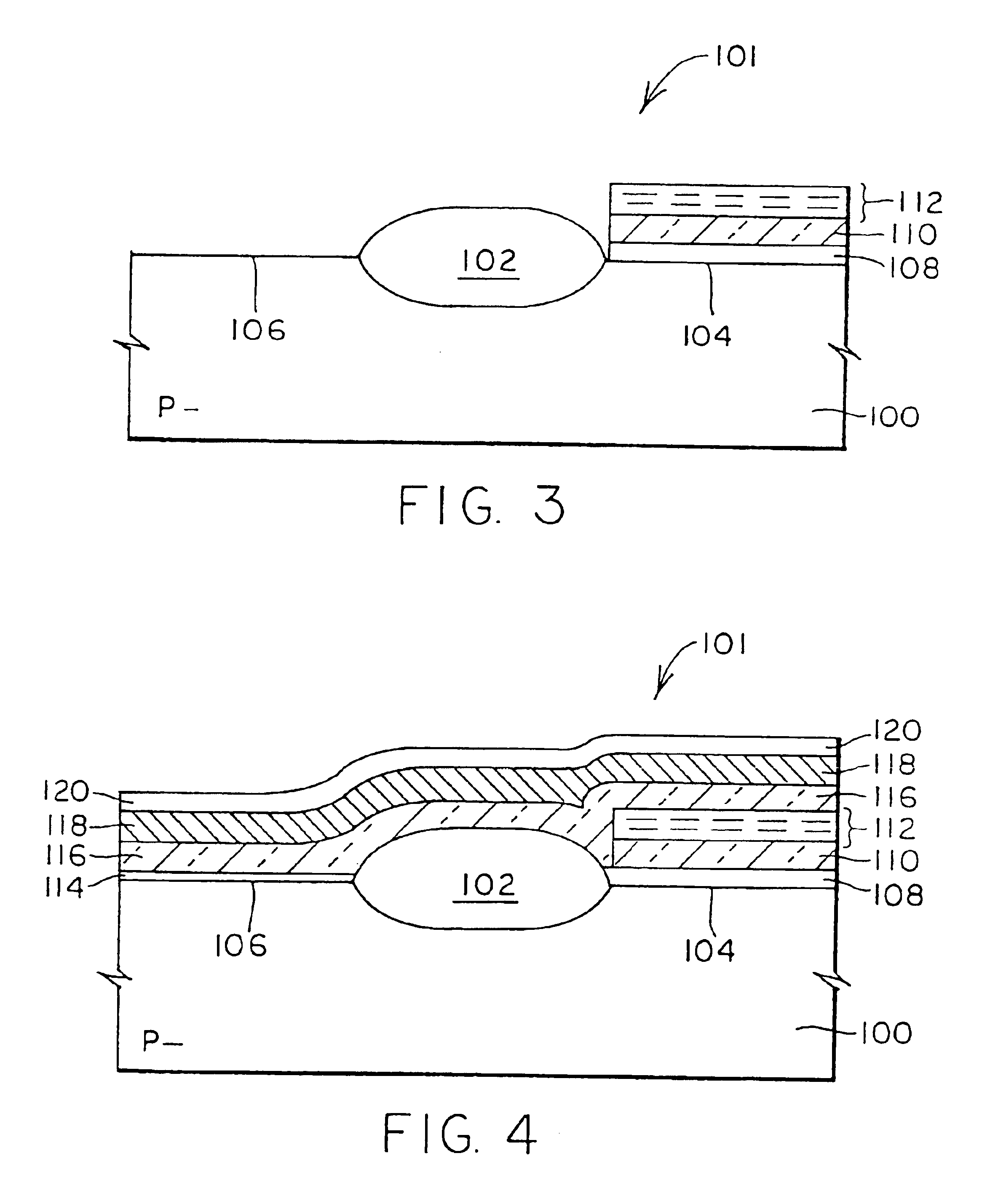
In another respect, disclosed is a method of fabricating a tungsten polycide
interconnection layer in a fully integrated
CMOS device having embedded analog sections and non-
volatile memory sections. In one exemplary embodiment, the method may include first depositing a layer of
amorphous silicon by, for example, low pressure
chemical vapor deposition (“LPCD”), subsequently
doping the deposited layer by, for example,
ion implantation, followed by annealing the deposited and doped layer using, for example, RTP to activate the
dopant and to reduce damage. The method may next include depositing a tungsten silicide layer on the doped
amorphous silicon by, for example, using PVD followed by RTP of the tungsten silicide layer in a
nitrogen environment to form a tungsten-based polycide structure. The method may next include depositing a silicon-rich oxynitride layer onto the tungsten-based polycide structure to serve as a polycide ARL for the patterning process using, for example, PECVD deposition. Non-volatile memory and control gate polycide stack structures may next be fabricated, for example, by patterning the tungsten-based polycide structure using
photolithography followed by reactive
ion etch (“RIE”) processes, and a
thin oxide may be subsequently grown on the sidewalls of non-volatile memory and control gate polycide stacks, for example, within a furnace tube. Source and drain areas may next be n-doped and / or p-doped to provide desired functionality. The method may next include depositing an oxide spacer layer using, for example, PECVD
tetraethyl orthosilicate (“TEOS”) deposition. The spacer layer may next be removed and over-etched from the top of the polycide and from the source and drain areas using, for example, RIE. Densification of the spacer and tungsten-based polycide structure may then be accomplished using RTP and a non-oxidizing environment in order to prevent polycide oxidation induced peeling.

