Electronic device and electronic apparatus

a technology of electronic equipment and electronic components, applied in the direction of device material selection, solid-state devices, impedence networks, etc., can solve the problems of low crystallization efficiency, low efficiency, and low cost of oxide ceramic substrates, and achieve high performan

Inactive Publication Date: 2005-02-01
SEIKO EPSON CORP
View PDF17 Cites 16 Cited by
  • Summary
  • Abstract
  • Description
  • Claims
  • Application Information

AI Technical Summary

Benefits of technology

[0024]According to the present invention, by including a suitable inorganic amorphous layer or an organic solid layer, as well as an oxide thin layer formed on the inorganic amorphous layer or the organic solid layer, and furthermore, by including a perovskite-type oxide thin film grown epitaxially on the oxide thin layer, and by using a suitable substrate including an inorganic amorphous layer or an organic layer, it is possible to provide an electronic device having a perovskite-type oxide thin film grown epitaxially in a desired direction on the inorganic amorphous layer or the organic solid layer. Furthermore, a high performance electronic device such as a surface acoustic device, a ferroelectric memory device, or a piezoelectric device can be provided by further incorporating such a device into an integrated circuit. Further, according to the present invention, a high performance electronic apparatus comprising any of the above electronic devices is provided.

Problems solved by technology

In an oriented film, packing density is tower than that in an epitaxial film, in-plane orientation is not as uniform, and crystallization is not as fully controlled.
Even though oxide ceramics such as SrTiO3 are normally used as a single crystal substrate, the cost of oxide ceramic substrates is generally high, and fabrication of large substrates of 3 inches or more in diameter is difficult depending on the types.
Even though a technology to grow a perovskite-type oxide thin film epitaxially on a silicon substrate is highly valuable in terms of cost and other factors, the technology alone cannot accomplish the desired integration with semiconductor devices.
Also, when a piezoelectric device such as an actuator is fabricated, a perovskite-type oxide thin film must be formed on a thermally oxidized film of a silicon oxide as well, so that a technology to form a perovskite-type oxide thin film on a silicon substrate alone is not sufficient.
There are examples of forming perovskite-type oxide thin films on a crystallized film of platinum or the like formed on an amorphous silicon oxide film; however, even though oriented films can be obtained in such cases, epitaxial films cannot be obtained.
As described in Japanese Unexamined Patent Application, First Publication No. 9-100125, there is an example of forming KNbO3 on an amorphous substrate; however, what is obtained is an oriented film, and obtaining an epitaxial film is still difficult.
It is difficult, furthermore, to grow a crystal in a desired orientation direction.

Method used


Image

  • Electronic device and electronic apparatus
  • Electronic device and electronic apparatus
  • Electronic device and electronic apparatus

Examples


example 1

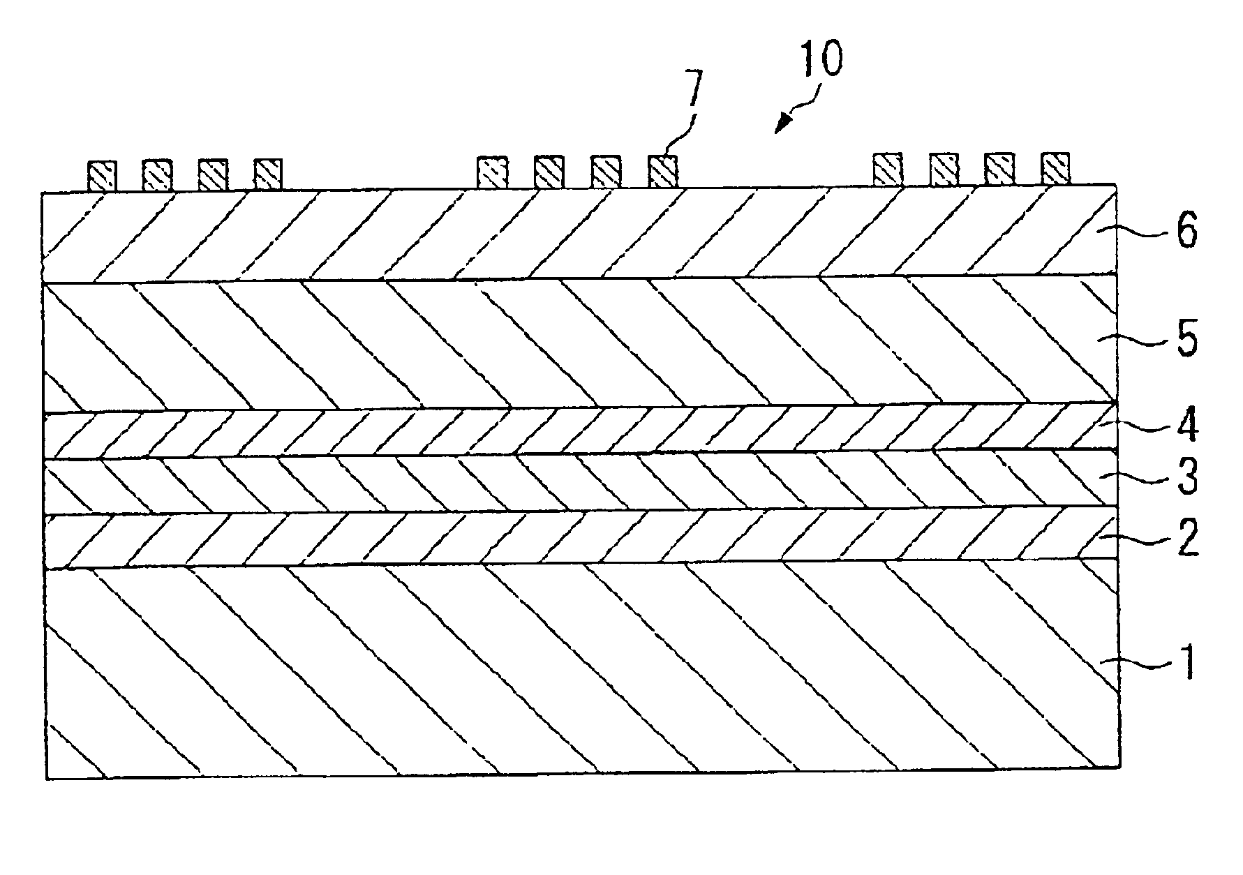
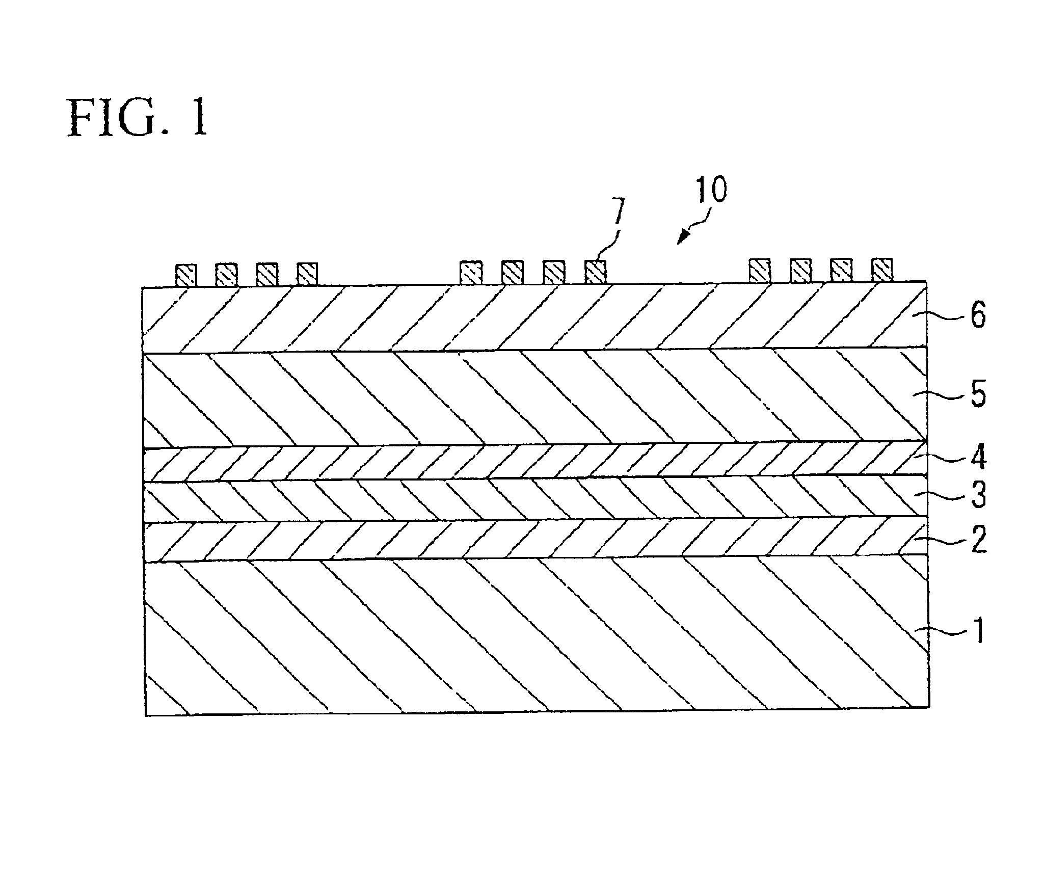
[0100]FIG. 1 is a cross sectional view of a surface acoustic device 10 in Example 1 of the present invention. The device 10 is comprised of a substrate 1, an amorphous layer 2, an oxide thin layer 3, an oxide thin layer 4, a piezoelectric thin film 5, a thin film 6 of an oxide or a nitride as a protective layer, and an electrode 7.

[0101]Fabrication processing of the surface acoustic device having the configuration above of the present invention is specifically described. A silicon substrate, on which a polycrystalline diamond thin film of thickness of 20 μm is formed, is used as a substrate 1. First, a SiO2 amorphous layer 2 is formed on the substrate 1 by using a laser ablation method. Next, a CeO2 thin film as an oxide thin layer 3 is formed similarly on the amorphous layer 2 by using a laser ablation method with an ion beam assist. With an oxygen plasma of 0.13 Pa (10−4 Torr) and a substrate temperature of 500° C., a CeO2 thin film of (100) orientation was formed. By examining in...

example 2

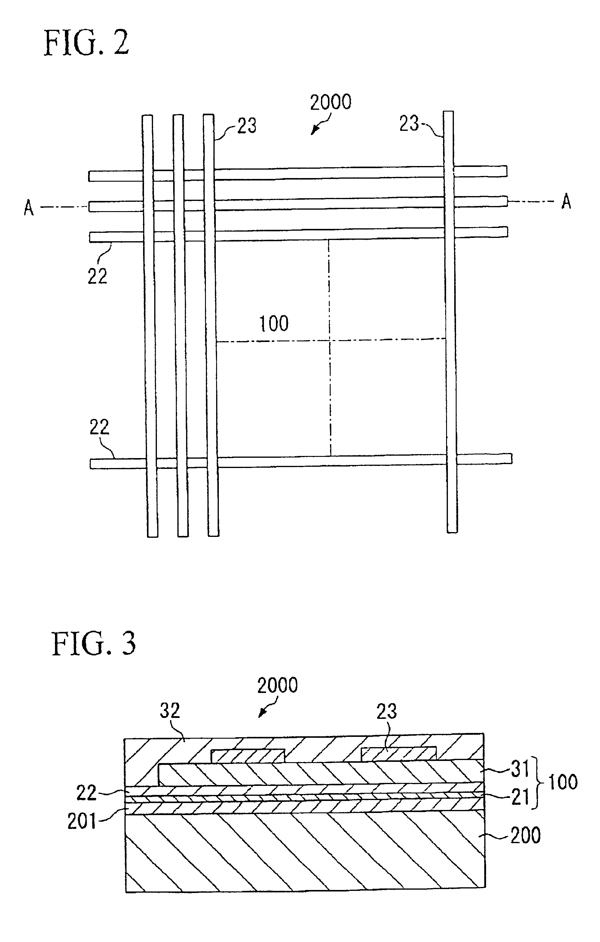
[0116]FIG. 2 is a schematic plan view of a ferroelectric memory device (a type of electronic device of the present invention) in Example 2 of the present invention. FIG. 3 is a partial schematic cross sectional view along A—A of FIG. 2

[0117]The ferroelectric memory devices of the Example 2 of the present invention having a matrix type memory cell array 100 with superior integration have a structure of forming the memory cell array 100 on a peripheral circuitry 200 containing MOS transistors for selecting a memory cell. The peripheral circuitry 200 contains various circuits in order to write or read data selectively from or to a memory cell. As shown in FIG. 3, the memory cell array 100 was formed on and in contact with the peripheral circuitry 200. Here, the top section of the peripheral circuitry 200 was a SiO2 amorphous layer of an interlayer insulating film acting as a protective layer at the same time. Consequently, the memory cell array 100 must be formed on the SiO2 amorphous ...

example 3

[0124]FIG. 4 is a schematic cross sectional view of a SAW oscillator in Example 3 of the present invention. The SAW oscillator comprises an oscillation circuit 300 and a SAW resonator 301. The reference numeral 310 refers to an oxide thin layer; reference numeral 311 refers to a perovskite-type oxide; reference numeral 312 refers to a piezoelectric thin film; reference numeral 313 refers to a thin film as a protective layer; and reference numeral 314 refers to an electrode. The uppermost section of the oscillation circuit 300 is a SiO2 amorphous layer 303 of an interlayer insulating film acting as a protective layer at the same time. Consequently, the SAW resonator 301 must be formed on the SiO2 amorphous layer 303; however, a piezoelectric thin film 312 must be grown epitaxially in order to obtain a SAW resonator 301 having good performance.

[0125]The fabrication process of the SAW resonator 301 is described by referring to FIG. 4, which is similar to the one described in Example 1....


PUM

PropertyMeasurementUnit
diameteraaaaaaaaaa
thicknessaaaaaaaaaa
temperatureaaaaaaaaaa

Abstract

Performance of an electronic device is highly improved by epitaxially growing a perovskite-type oxide thin film on an inorganic amorphous layer or an organic solid layer in a desired direction; and furthermore, a high performance electronic device is provided by incorporating the electronic device into an integrated circuit, wherein oxide thin layers are formed on the inorganic amorphous layer or the organic solid layer, and the perovskite-type oxide thin film is grown epitaxially on the oxide layer, the oxide thin layers being able to be at least one of strontium oxide, magnesium oxide, cerium oxide, zirconium oxide, yttrium stabilized zirconium oxide, and strontium titanate; and as the perovskite-type oxide thin film, the perovskite-type oxide thin film being a piezoelectric or ferroelectric material, for example, is used.

Description

BACKGROUND OF THE INVENTION[0002]1. Field of the Invention[0003]The present invention relates to an electronic device, especially, a ferroelectric device, a surface acoustic device, and a piezoelectric device, based on a perovskite-type oxide thin film grown epitaxially on an oxide thin layer on an inorganic amorphous layer or an organic solid layer, and an electronic apparatus comprising the electronic device.[0004]2. Description of the Related Art[0005]Conventionally, when a perovskite-type oxide thin film is grown epitaxially, a single crystal substrate or a crystallized buffer layer is chosen by considering lattice matching with a perovskite-type oxide to be grown epitaxially. For example, for a surface acoustic device using a perovskite-type oxide thin film, as described in Japanese Unexamined Patent Application, First Publication No. Hei 2000-278084, good properties have been obtained by growing a potassium niobate (described as “KNbO3” hereafter) thin film having a high elect...

Claims


Application Information

Patent Timeline
Patent Type & Authority Patents(United States)
IPC IPC(8): H03H9/02H01L21/02H01L21/316H01L41/08H01L21/8246H01L27/105H01L41/09H01L41/18H01L41/187H03H9/17H03H9/25
CPCH03H9/174H03H9/02574H01L21/31691H01L28/56Y10S257/918H01L21/02164H01L21/02197H01L21/02189H01L21/02192H01L21/02172
Inventor IWASHITA, SETSUYAHIGUCHI, TAKAMITSUMIYAZAWA, HIROMU
Owner SEIKO EPSON CORP
Why Eureka
Try Eureka