Microfabrication of organic optical elements

Inactive Publication Date: 2005-02-15
3M INNOVATIVE PROPERTIES CO
View PDF73 Cites 98 Cited by
  • Summary
  • Abstract
  • Description
  • Claims
  • Application Information

AI Technical Summary

Benefits of technology

The present invention provides three-dimensional, polymeric, optical circuits and elements with excellent dimensional and optical stability over wide temperature ranges. The optical characteristics, e.g., index of refraction, are also stable,

Problems solved by technology

Both approaches are labor intensive and costly.
The cost increases proportionately with the number of fibers used due to the additional labor needed to fuse or attach each individual fiber.
Such intensive labor inhibits mass production of these devices.
A further problem results from the mismatch in shape of the optical modes in the glass fiber and the integrated optical device.
This mismatch tends to cause insertion losses when a fiber is butt coupled to an integrated optical device.
The manufacture of other three dimensional, micro-optical elements has been quite challenging.
However, the range of shapes that can be made using lithography are limited by a number of factors including surface tension effects.
Photolithography also is limited to the fabrication of elements whose optical axis is normal to the substrate upon which the element is fabricated.
It is difficult, for instance, to make elements with accurate undercuts using photolithography.
Alignment of the layers during assembly to form the la

Method used


Image

  • Microfabrication of organic optical elements
  • Microfabrication of organic optical elements
  • Microfabrication of organic optical elements

Examples


example 1

Example 1

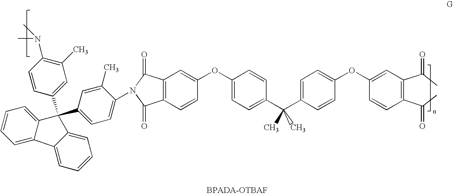
A solution of photodefinable polyimide G

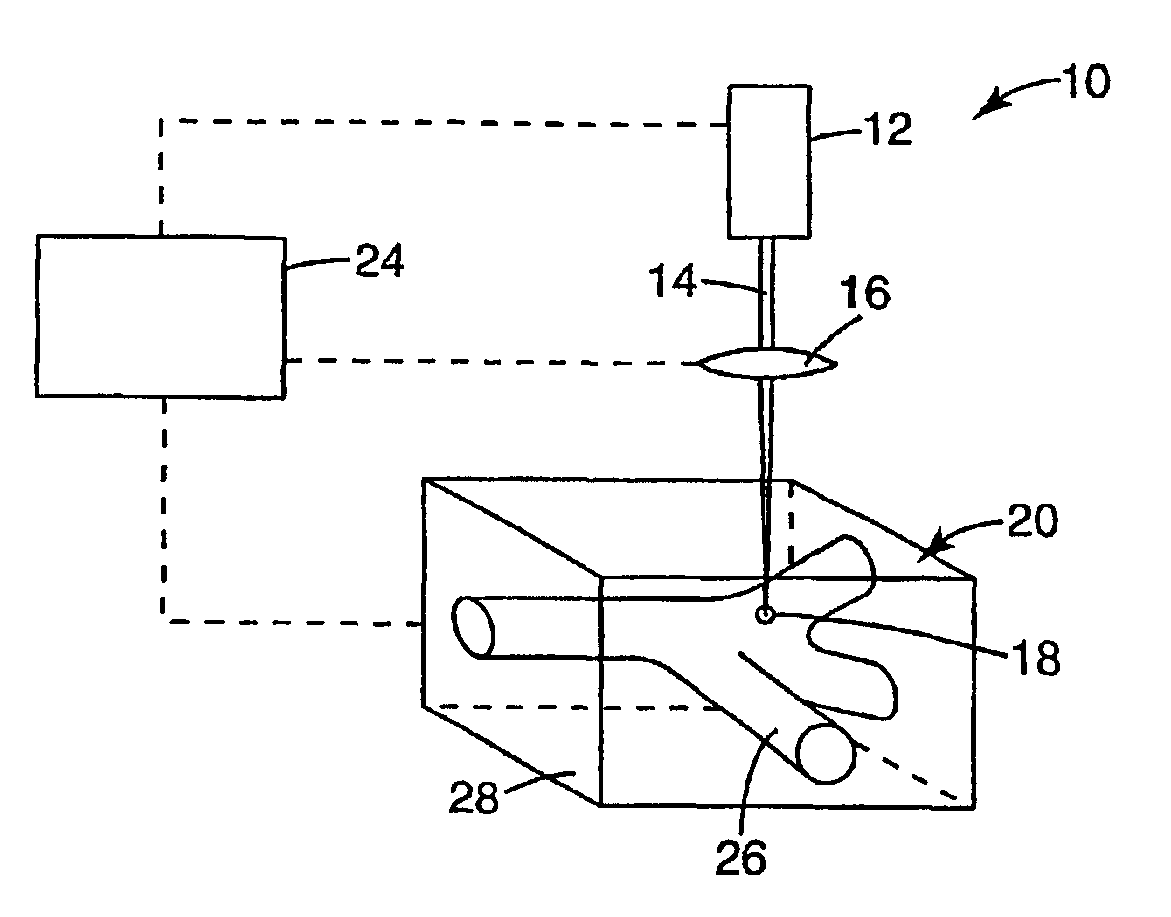
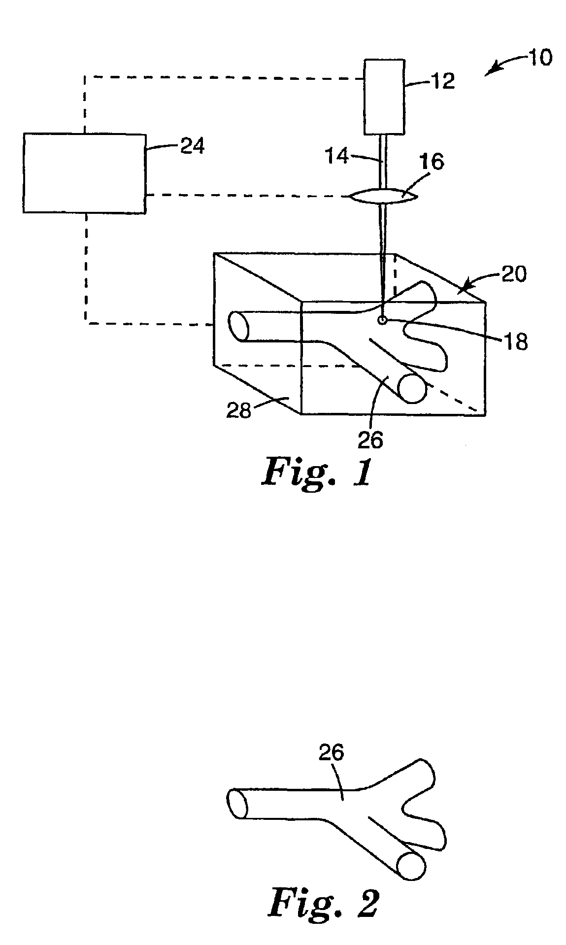
and two-photon photosensitization system including 4,4′-bis(diphenylamino)-trans-stilbene (1 weight %, based on solids) and diphenyliodonium hexafluorophosphate (1 weight % based on solids) is prepared in a suitable solvent (NMP) at approximately 20% solids and coated on a silicon wafer by knife coating to about 200-300 microns wet thickness. The coating is dried overnight (about 16 hrs) in an oven at about 50° C. Exposure and patterning is performed using a two-photon microscope with a Ti:Sapphire laser operating at the two-photon absorption maximum of 4,4′-bis(diphenylamino)-trans-stilbene, 700 nm, and the light is focused through a 40× objective with a focal length of 4.48 mm and a numerical aperture of 0.65. The pattern constituting the optical element is produced by manipulation of the substrate under the fixed focal point of the beam, accomplished by means of X-Y-Z servo-feedback-controlled translation stages equipped with high...

example 2

In this example, the following abbreviations are used:

MPS I—multiphoton photo sensitizer I prepared as described below.

DPI PF6—diphenyliodonium hexafluorophosphate, which can be made essentially as described in column 4 of U.S. Pat. No. 4,394,403 (Smith), using silver hexafluorophosphate.

Durimide 7520—a photoimageable polyimide, 40 weight % solids in NMP, available from Arch Chemicals, E. Providence, R.I.

NMP—1-methyl-2-pyrrolidinone, available from Aldrich, Milwaukee, Wis.

TMSPMA—3-(trimethylsilylpropyl) methacrylate, available from Aldrich, Milwaukee, Wis.

PGMEA—propylene glycol methyl ether acetate, available from Aldrich, Milwaukee, Wis.

(a) Reaction of 1,4-bis(bromomethyl)-2,5-dimethoxybenzene with triethyl phosphite:

1,4-Bis(bromomethyl)-2,5-dimethoxybenzene was prepared according to the literature procedure (Syper et al, Tetrahedron, 39, 781-792, 1983). The 1,4-bis(bromomethyl)-2,5-dimethoxybenzene (253 g, 0.78 mol) was placed into a 1000 mL round bottom flask. Triethyl phosphite ...

example 3

Preparation of Cylindrical Lenses:

An 85 micron film prepared as in Example 2 was mounted on a computer-controlled 3-axis stage, and the output of a Ti:Sapphire laser (part of a “Hurricane” system manufactured by Spectra-Physics Laser) (800 nm, 100 fs pulse, 29 mW, 80 MHz), equipped with a 40× objective lens (numeric aperature of 0.65), was focused into the film. The stage was programmed to move so as to produce a series of cylindrical lens images, each 100 micrometers wide by 200 micrometers long by 80 micrometers tall, with a radius of curvature of 100 micrometers. The sample was scanned under the focused beam at a rate of 1 mm / s to produce the structures. After development with cyclohexanone / 1-methyl-2-pyrrolidinone (4 / 1), a series of three-dimensional cylindrical lenses were obtained on a silicon wafer with the lens curvature normal to the silicon wafer substrate.


PUM

PropertyMeasurementUnit
Temperatureaaaaaaaaaa

Abstract

Method of fabricating an optical element. A photodefinable composition is provided that includes (i) a hydrophobic, photodefinable polymer, said photodefinable polymer having a glass transition temperature in the cured state of at least about 80° C.; and (ii) a multiphoton photoinitiator system comprising at least one multiphoton photosensitizer and preferably at least one phtoinitiator that is capable of being photosensitized by the photosensitizer. One or more portions of the composition are imagewise exposed to the electromagnetic energy under conditions effective to photodefinably form at least a portion of a three-dimensional optical element.

Description

FIELD OF THE INVENTIONThis invention relates to the use of multiphoton-induced photodefining methods for fabricating optically functional elements (e.g., waveguides, diffraction gratings, other optical circuitry, lenses, splitters, couplers, ring resonators, and the like) that find particular utility in optical communication systems.BACKGROUND OF THE INVENTIONOptical interconnects and integrated circuits may be used, in one application, optically connect one or more optical fibers to one or more remote sites, typically other optical fibers. For example, where light is carried by one or more input fiber(s), the light may be transferred to, split between, or merged into one or more remote sites. Active or passive devices within the optical integrated circuit may also modulate or switch the input signal. Optical interconnects play an important role in fiber telecommunication, cable television links, and data communication. A waveguide is a type of optical interconnect.For the most part...

Claims


Application Information

Patent Timeline
IPC IPC(8): G02B6/13G02B6/138B29C67/00G02B3/00G02B3/06G02B5/18G02B6/122G03F7/038G03F7/20
CPCB29C67/0055G02B3/06G03F7/2053G02B6/13G02B6/138G03F7/0387G02B6/1221B29L2011/0075B29C64/135B33Y70/00B33Y10/00B29C64/188G02B6/00G03C1/73
Inventor DEVOE, ROBERT J.LEATHERDALE, CATHERINE A.MAO, GUOPINGFLEMING, PATRICK R.KALWEIT, HARVEY W.
Owner 3M INNOVATIVE PROPERTIES CO
Why Eureka
Try Eureka