
Photodiode, optical receiver device including the same, and method of making the photodiode

Inactive Publication Date: 2006-06-06
SUMITOMO ELECTRIC IND LTD
View PDF4 Cites 21 Cited by
  • Summary
  • Abstract
  • Description
  • Claims
  • Application Information

AI Technical Summary

Benefits of technology

[0034]The passivation film is composed of a hard and thin inorganic substance. The protective layer may be composed of a substance different from that for the passivation film, for example, a polymer. The polymer protective layer can be formed by spin-coating and curing a liquid raw material. Thereby a protective layer with a required thickness can be readily formed and does not generate internal stress in the underlying passivation film even if the thickness of the protective layer is thick. The protective layer may comprise any one selected from the group consisting of a polyimide resin, a fluorinated polyimide resin, polymethyl methacrylate resin, an epoxy resin, and an ultraviolet-curable resin. The protective layer must be thick. Preferably, the thickness of the protective layer may be 10 times to 100 times the thickness of the passivation film. Preferably, the protective layer may have a thickness in the range of 5 μm to 50 μm.
[0043]Since a number of PD chips can be mounted onto the Si wafer in the wafer fabrication process, the production cost can be further reduced. Consequently, high-performance surface mounting photodiode modules with low dark current can be provided at reduced costs.

Problems solved by technology

However, such a photodiode module inevitably requires axial alignment and use of an expensive metal package, which results in high material and process costs and bulkiness.
However, only a PD mounting step can precede the chip-dicing step.
It is difficult to transfer a wired wafer after wire bonding and to scribe it by using a scriber without damaging the wires.
We will now forecast new problems that would arise if the PD was mounted in a step of the wafer fabrication process for the surface mounting PD module, although no example of a scribing step after mounting of the PD onto the Si wafer is actually known.
Since the Si wafer has a considerable thickness, chips may be damaged by the mechanical dicing and will be contaminated by dicing chips.
Although the contaminations such as dicing chips and cutting solution residue can be removed by cleaning to some extent, sticky fine contaminations cannot be easily removed.
If the PD chips are fixed to a wafer before dicing, the PD chips will also be subjected to shock from dicing.
When dicing is performed along the scribing lines on the Si wafer, chips may damage the passivation films of the PD chips.
Removal of the contaminations such as sodium ions adhered to the PD chips is extremely difficult.
Such contaminations may reach the ends of the p-n junction and may impair the function of the p-n junction.
As a result, a dark current that flows when no light is incident in a reverse bias mode may increase, thus increasing noise.
If so, a dark current generated by leakage of carriers from the p-n junction increases, resulting in an increase in noise and deterioration of receiving performance.
Such a dark current may cause malfunction of the device at high environmental temperatures, since the thermal changes of dark current is significant.
As a result of the generation of the inversion layer, part of the p-n junction is extremely thinned and causes an increase in dark current due to breakdown.
The noisy dark current causes deterioration of the receiving characteristics and inhibits receiving high-frequency pulse signals.
Such a process has never been performed, however; hence, the above problems are not actually observed.
Dicing involves mechanical cutting in which a lubricant oil and an abrasive agent (including abrasive powder and chemical agent) are applied and a rotating blade is brought into direct contact with the wafer; hence, the PD will be significantly contaminated.

Method used


Image

  • Photodiode, optical receiver device including the same, and method of making the photodiode
  • Photodiode, optical receiver device including the same, and method of making the photodiode
  • Photodiode, optical receiver device including the same, and method of making the photodiode

Examples


first embodiment (rear illuminated type pd : figs.1 and 2)

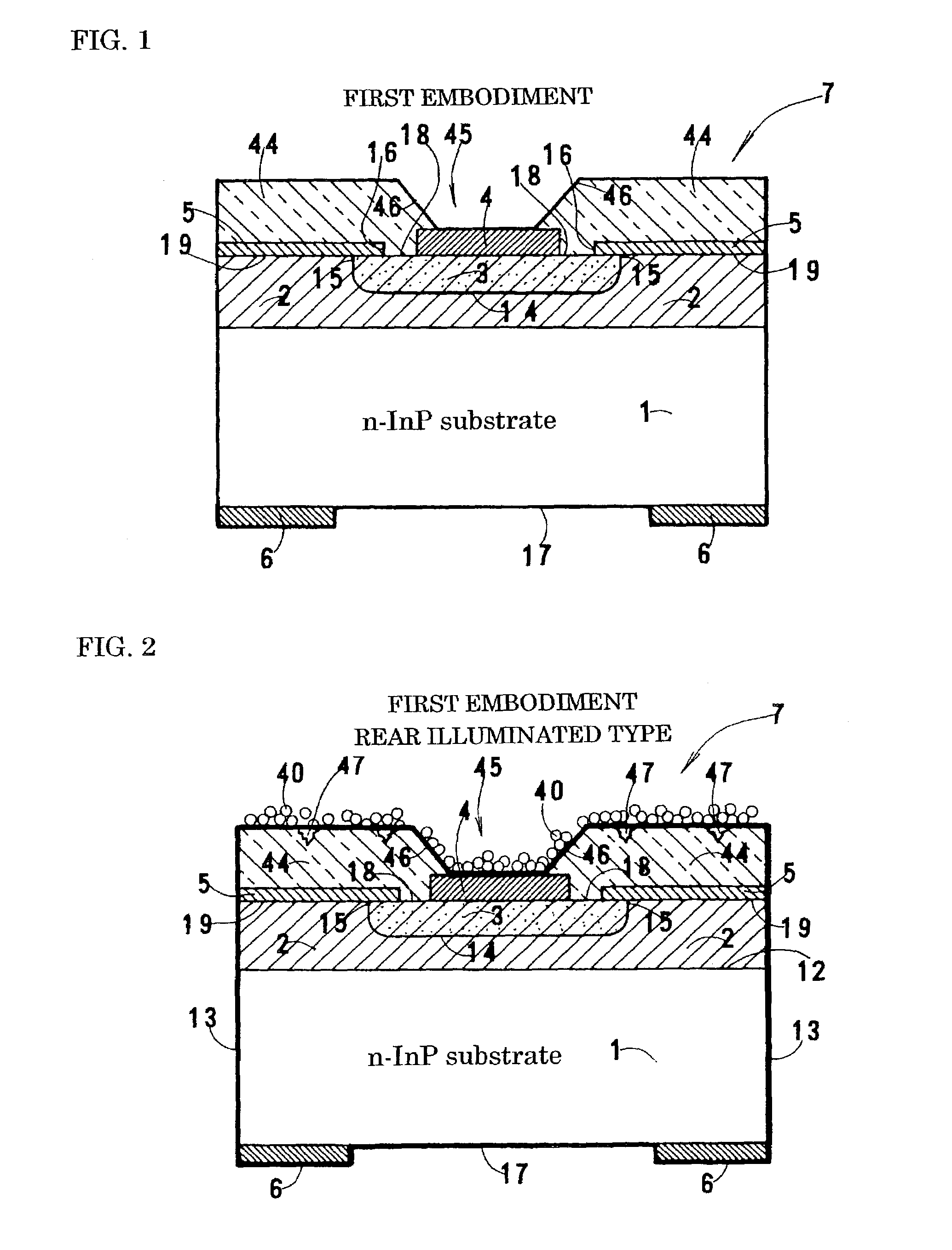
FIRST EMBODIMENT (REAR ILLUMINATED TYPE PD: FIGS. 1 AND 2)

[0073]FIG. 1 is a cross-sectional view of a rear illuminated PD provided with a protective layer according to a first embodiment of the present invention. An n-InGaAs absorption layer 2 is deposited on an n-InP substrate 1 by epitaxial growth. The center of the n-InGaAs absorption layer 2 is a p-type region 3 formed by zinc diffusion. A dish-shaped p-n junction 14 is formed in the n-InGaAs absorption layer 2. A p-electrode 4 is formed on the center of the p-type region 3. The p-electrode 4 is made of a titanium / gold alloy. A passivation film 5 is formed on the peripheral region of the top face of the p-type region 3. The passivation film 5 also covers the peripheral regions 19 of the top face of the n-InGaAs absorption layer 2. The end 15 of the p-n junction is located under the passivation film 5 and away from the inner end 16 thereof. An annular n-electrode 6 is formed on the rear face (bottom face) of the n-InP substrate 1...

second embodiment (rear illuminated type pd : diffusion shielding layer , fig.3)

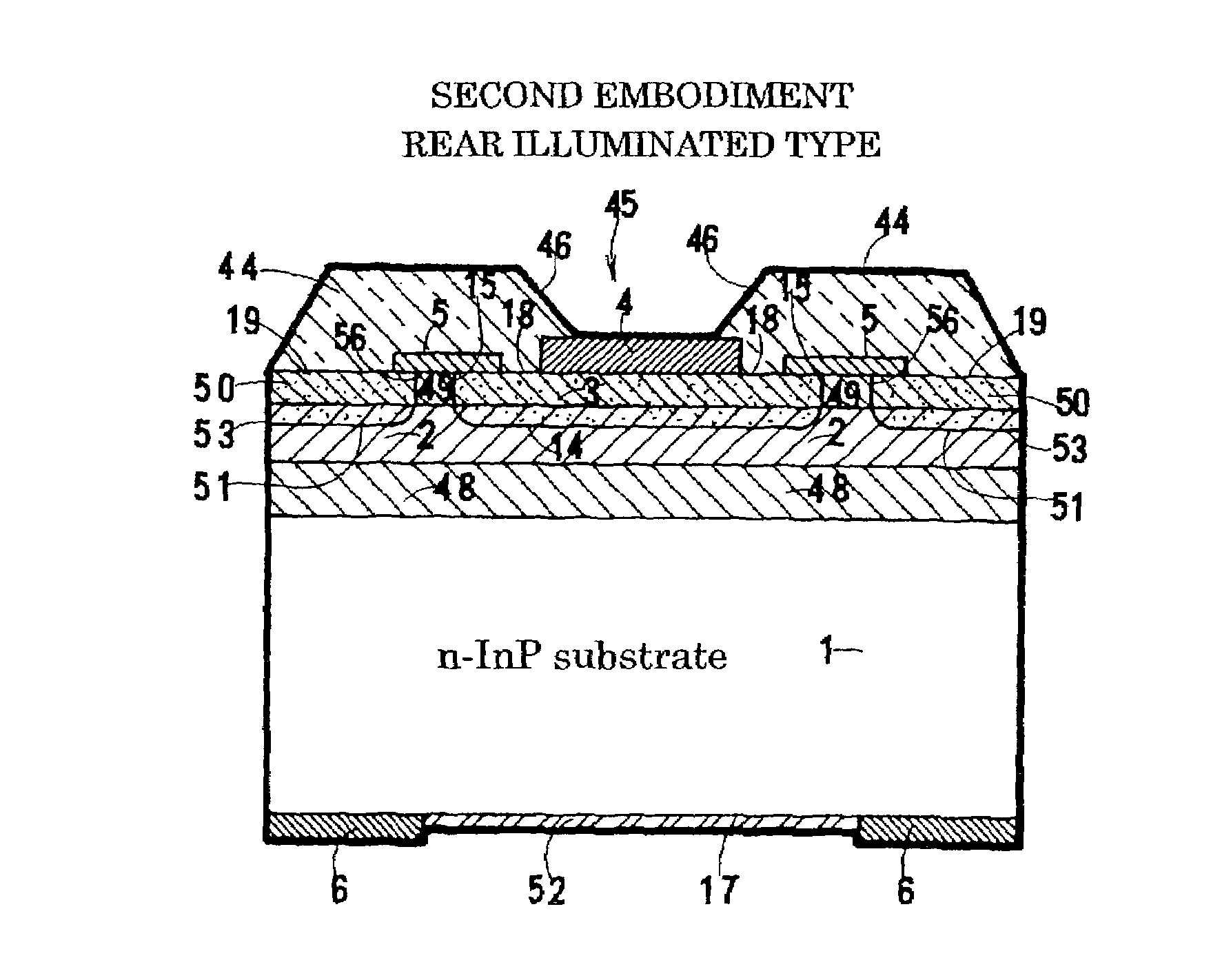
SECOND EMBODIMENT (REAR ILLUMINATED TYPE PD: DIFFUSION SHIELDING LAYER, FIG. 3)

[0082]FIG. 3 is a cross-sectional view of a rear illuminated PD provided with a protective layer and a diffusion shielding layer according to a second embodiment of the present invention. A cap layer and a buffer layer are provided in the crystal structure, and an annular p-type layer as the diffusion shielding layer is provided at the peripheral portion of the top face of the PD.

[0083]An n-InP buffer layer 48, an n-InGaAs absorption layer 2, and an n-InP cap layer 49 are deposited on an n-InP substrate 1 by epitaxial growth. The n-InP buffer layer 48 is deposited at a low temperature for improving the crystallinity of the n-InGaAs absorption layer 2. The n-InP cap layer 49 improves the ohmic contact between a p-type region and a p-electrode. The n-InP cap layer 49 is called a window layer for receiving light in a front illuminated type, although it is called a cap layer in a rear illuminated type since n...

third embodiment (front illuminated type pd : diffusion shielding layer and antireflective film , fig.4)

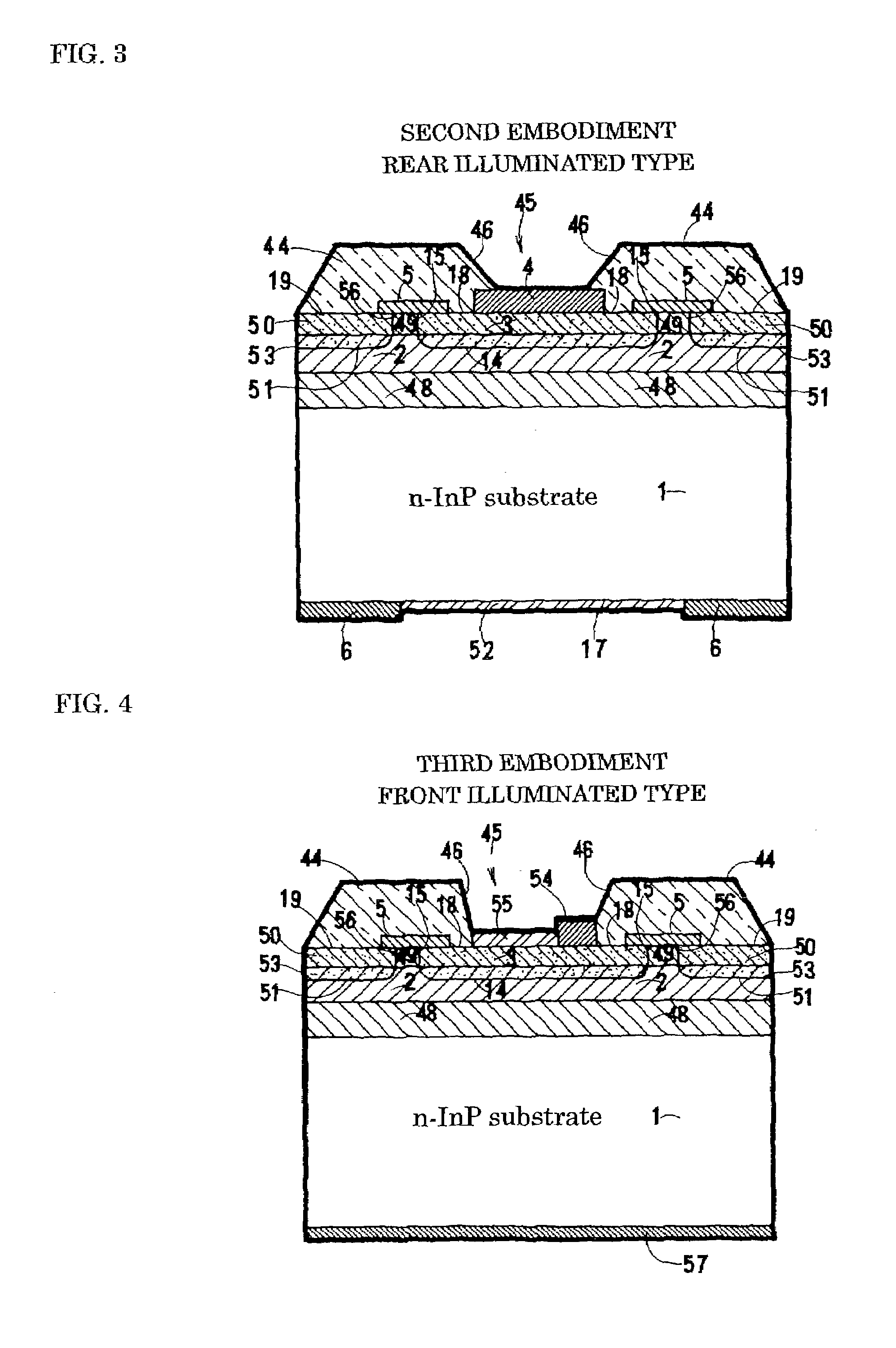
THIRD EMBODIMENT (FRONT ILLUMINATED TYPE PD: DIFFUSION SHIELDING LAYER AND ANTIREFLECTIVE FILM, FIG. 4)

[0095]The present invention is also applicable to a front illuminated photodiode. FIG. 4 is a cross-sectional view of a front illuminated photodiode having a protective layer and a diffusion shielding layer according to a third embodiment of the present invention. A small dot p-electrode is provided on the top face of the PD such that light enters the top face through the opening in the center of the top face, which is covered with an antireflective film. The rear face, on which light is not to be incident, is covered by an n-electrode. In this embodiment, the diffusion shielding layer and a window or cap layer are provided. The diffusion shielding layer and the window layer may be omitted.

[0096]An n-InP buffer layer 48, an n-InGaAs absorption layer 2, and an n-InP window or cap layer 49 are epitaxially deposited on an n-InP substrate 1. An annular passivation film 5 is formed on t...


PUM


Abstract

A photodiode (PD chip) includes a substrate, an absorption layer, a p-n junction in the absorption layer, a passivation film for protecting the end of the p-n junction, a p-electrode, and an n-electrode. The passivation film is covered with a protective layer composed of an insulative resin and having a thickness larger than that of the passivation film such that the passivation film of the PD chip fixed to the Si wafer and hence the p-n junction are not damaged or contaminated when an Si wafer including a number of horizontally and vertically arranged chip units, each having a V-groove for fixing an optical fiber, a marker, and a metallized pattern, is diced. Thus, a low-cost optical receiver module that does not generate dark current can be produced.

Description

BACKGROUND OF THE INVENTION[0001]1. Field of the Invention[0002]The present invention relates to photodiodes having p-n junctions, and particularly relates to a photodiode suitable for optical communication, an optical receiver device including the photodiode, and a method of making the photodiode.[0003]2. Description of the Related Art[0004]A typical widely used photodiode module is accommodated in a coaxial type metal package with a lead pin. A front illuminated photodiode ID) chip is fixed to the surface of a stem. A lens and an optical fiber are fixed in axial alignment on the PD chip, and the module is sealed hermetically. Signal light having propagating through the optical fiber is converged by the lens and is incident on the top of the PD, which converts the light into a photocurrent. The device is tightly sealed in the metal package to ensure stable characteristics and a prolonged lifetime with high reliability. However, such a photodiode module inevitably requires axial ali...

Claims


Application Information

Patent Timeline
IPC IPC(8): H01L31/06G02B6/42G02B6/30H01L31/0216H01L31/0232H01L31/10
CPCH01L31/02162G02B6/4202G02B6/4214
Inventor YAMABAYASHI, NAOYUKIKUHARA, YOSHIKI
Owner SUMITOMO ELECTRIC IND LTD
Features
  • Generate Ideas
  • Intellectual Property
  • Life Sciences
  • Materials
  • Tech Scout
  • Unparalleled Data Quality
  • Higher Quality Content
  • 60% Fewer Hallucinations
Learn More