
Resin composition, heat-resistant resin paste and semiconductor device using them and method for manufacture thereof

a technology of resin composition and heat-resistant resin, which is applied in the direction of solid-state devices, machines/engines, group 5/15 element organic compounds, etc., can solve the problems of warpage of substrates, warpage of frames, and small residual stress,

Inactive Publication Date: 2006-06-13
HITACHI CHEM CO LTD
View PDF7 Cites 25 Cited by
  • Summary
  • Abstract
  • Description
  • Claims
  • Application Information

AI Technical Summary

Benefits of technology

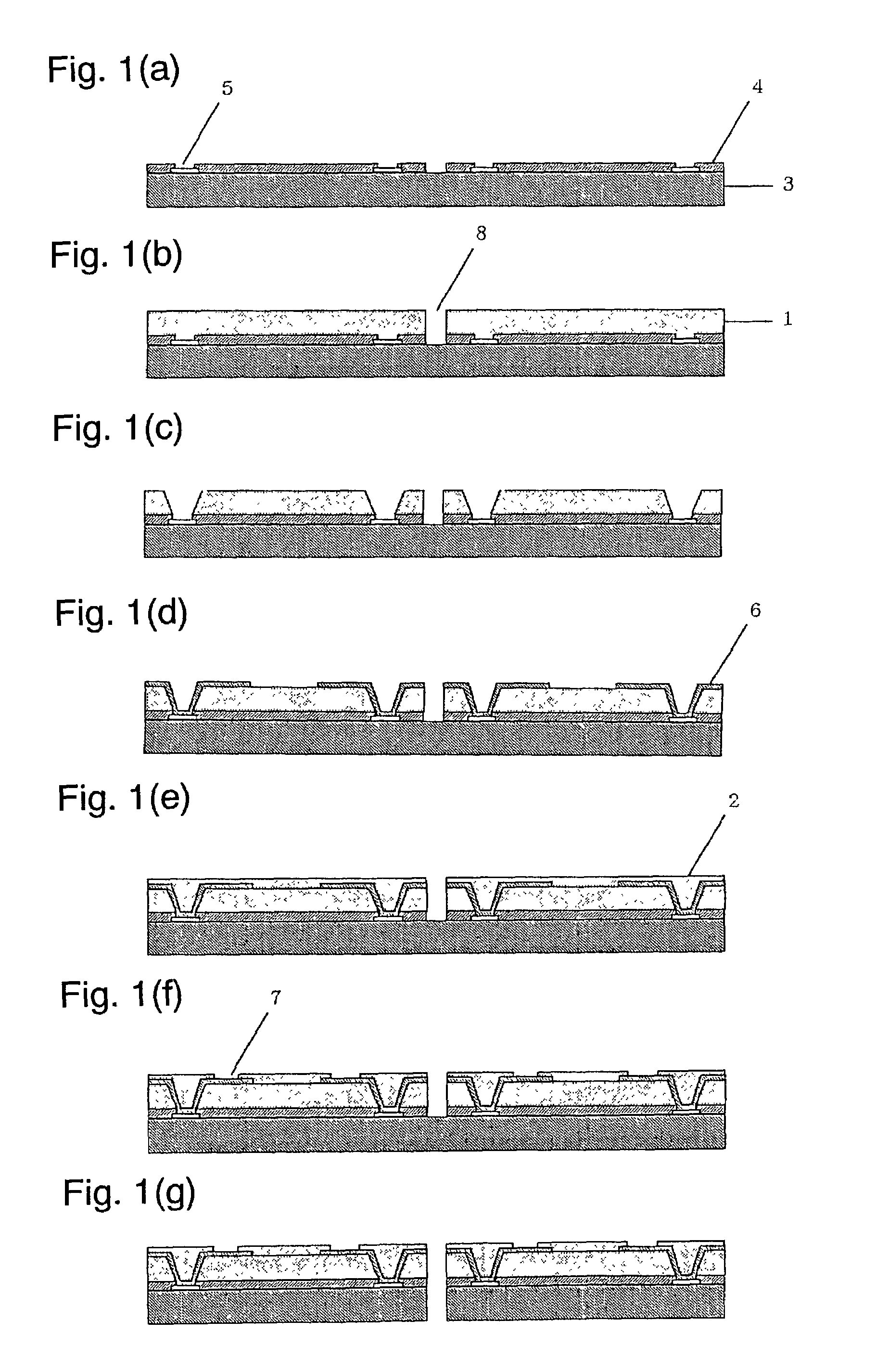
[0037]A method of producing a semiconductor device according to the present invention further comprises a step of forming a plural number of resin layers on a semiconductor wafer on which a first wiring layer has been formed by printing a resin having an elasticity at 25° C. of 0.2 to 3.0 GPa, a glass transition temperature of 180° C. or higher and a 5% weight-loss temperature of 300° C. or higher; a step of forming a second wiring layer on the resin layer which is electrically connected to an electrode on the semiconductor wafer; a step of forming a plural number of protective layers of the second wiring layer by printing the above resin on the second wiring layer; a step of providing a through hole(s) at the protective layer of the second wiring layer penetrating to of the second wiring layer; and a step of forming an outer electrode terminal to the through hole(s); and a step of cutting the semiconductor wafer to obtain respective semiconductor devices.

Problems solved by technology

In particular, whereas the size of the whole parts is becoming small, a chip mounted thereon is becoming a large sized and thin so that a damage caused by the stress at the time of curing or after curing is likely caused.
In particular, for forming a product in which a plural number of bear chips are mounted on the same substrate like an IC card or a resin dam of a lead frame, a slight residual stress at the time of curing becomes a cause of breakage of wiring, warpage of a substrate or distortion of a frame.
For forming a product on which a plural number of bear chips are mounted on the same substrate like an IC chip or a resin dam of a lead frame, an epoxy resin, etc., has conventionally been used, but the resin has a large stress accompanied by shrinkage at curing so that breakage of wiring or occurrence of crack after curing becomes problems in a heat cycle test after curing or a solder reflow test.
Also, with regard to strain at the time of forming a resin dam on a lead frame, a mold resin is flown out from the portion at which strain occurs whereby there is a problem of molding failure at molding.
However, there are problems that adhesiveness is lowered or resin strength is lowered.
Also, in CSP (chip size package), a solder connecting portion is plastically deformed in a semiconductor device in a surface mounting type such as a bear chip packaging, by a stress caused by the difference of thermal expansion coefficients between a semiconductor element and a substrate, and when this is repeated, the device is broken by fatigue.
Moreover, in a bear chip practical packaging, there is no structure at the inside of the semiconductor to relax the stress so that a device to reduce the stress caused by the difference of the thermal expansion coefficients of the substrate has been carried out by providing an underfill resin layer between the semiconductor element and the substrate.
However, in the structure of relaxing a stress at the connecting portion by the height of the bump as mentioned above, the stress is rather concentrated to the bump itself so that there is a problem of causing connection failure.
Also, in the method of using the underfill resin layer in combination, a resin is required to fill in a narrow gap between the semiconductor device and the substrate so that a filling operation is troublesome.
Moreover, it is difficult to fill the resin uniformly in the whole portion of the gap so that there is a problem of lowering in production efficiency of the semiconductor device.
However, the low elasticity material used in μBGA is low elasticity but is poor in heat resistance so that it has low resistance to sputtering or plating whereby it cannot be applied to the wafer level CSP process as such.
On the other hand, it has been carried out an attempt to relax the stress by adding a monomer component having rubber elasticity to an epoxy resin to lower the elasticity (Japanese Provisional Patent Publication No. 48544 / 1986), but by using these components in combination, there is a problem of lowering heat resistance of the resin.
A thermoplastic resin having high heat resistance generally has high resin elasticity and mechanical strength but is brittle so that it is applied to electronic parts as such, there are high possibility of causing inconveniences such as occurrences of warpage of a substrate after curing or resin crack in a thermal shock test.
However, this method becomes a cause of lowering heat resistance of the resin itself so that it is not preferred.
However, these materials involve the problem that many voids or bubbles are remained at the filler interface at heating and drying so that film strength is weak.
Also, there are problems that elasticity is high and flexibility is poor.
Moreover, in the other polyimide paste, similar problems are involved.
In the spin coating method, there are problems in environmental point and cost that a coating efficiency of the heat-resistant resin solution is generally 10% or less (90% or more are lost without coating to the substrate), etc.
However, this heat-resistant resin has large elasticity so that there is a problem that it cannot be used as such as a stress relaxing material for relaxing the difference in thermal expansion coefficients of a silicon chip and the substrate.
Also, in the method of using a spin coating step when an insulating layer is formed on the wafer surface, there is much loss in a material to be used, and there is a problem that a cost becomes much expensive until a mass production technique is established.

Method used


Image

  • Resin composition, heat-resistant resin paste and semiconductor device using them and method for manufacture thereof
  • Resin composition, heat-resistant resin paste and semiconductor device using them and method for manufacture thereof
  • Resin composition, heat-resistant resin paste and semiconductor device using them and method for manufacture thereof

Examples


example 1

[0241]In a one-liter four-necked flask equipped with a thermometer, a stirrer, a nitrogen inlet tube, and a condenser equipped with an oil-water separator was charged 98.4 g (240 mmol) of 2,2-bis[4-(4-aminophenoxy)phenyl]propane (BAPP) under nitrogen atmosphere, and 700 g of N-methyl-2-pyrrolidone (NMP) was added thereto to dissolve the mixture. Next, while cooling the mixture not to exceed 20° C., 51.2 g (244 mmol) of trimellitic anhydride chloride (TAC) was added to the mixture. After stirring the mixture at room temperature for one hour, 30.3 g (300 mmol) of triethylamine was added while cooling the mixture not to exceed 20° C., and the resulting mixture was reacted at room temperature for 3 hours to produce a polyamic acid varnish. The resulting polyamic acid varnish was further subjected to dehydration reaction at 190° C. for 6 hours to produce a varnish of a polyether amide imide. This varnish of the polyether amide imide was poured into water and the resulting precipitates we...

example 2

[0247]Production of the resin composition and the semiconductor device, and the evaluations thereof were conducted in the same manner as in Example 1 except that, in a synthesis of a polyether amide imide which is soluble in a polar solvent at the room temperature, a diamine compound was changed to 93.3 g (216 mmol) of bis[4-(4-aminophenoxy)phenyl]phenyl]sulfone (BAPS) and 6.0 g (24 mmol)of 1,3-bis(aminopropyl)tetramethyldisiloxane. The results are shown in Table 1.

example 3

[0248]Production of the resin composition and the semiconductor device, and the evaluations thereof were conducted in the same manner as in Example 1 except that, in a synthesis of a polyether amide imide which is soluble in a polar solvent at the room temperature, a diamine compound was changed to 78.7 g (192 mmol) of 2,2-bis[4-(4-aminophenoxy)phenyl]propane (BAPP), 6.0 g (24 mmol) of 1,3-bis(aminopropyl)tetramethyldisiloxane and 4.8 g (24 mmol) of 4,4′-diaminodiphenyl ether, an acid compound was changed to 24.8 g (122 mmol) of isophthalic acid dichloride and 25.6 g (122 mmol) of trimellitic anhydride chloride. The results are shown in Table 1.


PUM

PropertyMeasurementUnit
particle sizeaaaaaaaaaa
thermal decomposition temperatureaaaaaaaaaa

Abstract

There are disclosed a resin composition comprising (A) a heat-resistant resin soluble in a solvent at room temperature, (B) a heat-resistant resin which is insoluble in a solvent at room temperature but becomes soluble by heating, and (C) a solvent; a heat-resistant resin paste further containing (D) particles or liquid state material D showing rubber elasticity; and a semiconductor device using the same and a method for producing the same.

Description

TECHNICAL FIELD[0001]This invention relates to a resin composition, a heat-resistant resin paste and a semiconductor device using these and a method of preparing the same, more specifically to a resin composition excellent in adhesive property, heat-resistance and flexibility, a heat-resistant paste which can provide a heat-resistant resin layer which is widely utilized as a coating material, adhesive and stress releasing material of a semiconductor device, is capable of optionally controlling an elasticity and has a little temperature dependency of the elasticity, and can provide such a heat-resistant resin film, and a semiconductor device using these and a method of preparing the same.BACKGROUND ART[0002]In recent years, electronic parts are becoming small sized and thin, and it is an important technical task to relax a stress with regard to a material applied to these parts. For example, with regard to a material which is directly coating the electronic parts, a high stress relax...

Claims


Application Information

Patent Timeline
Patent Type & Authority Patents(United States)
IPC IPC(8): C08L79/08H01L23/48G03F7/038H01L21/312H01L21/768H01L23/532
CPCG03F7/0387H01L21/02118H01L21/02126H01L21/02216H01L21/02282H01L21/312H01L21/3122H01L23/5329H01L2924/0002H01L2924/00C08L101/00
Inventor YANO, YASUHIROMATSUURA, HIDEKAZUNOMURA, YOSHIHIROMORISHITA, YOSHIISAKATA, TOUICHINISHIZAWA, HIROSHITANAKA, TOSHIAKIYASUDA, MASAAKIKANEDA, AIZOU
Owner HITACHI CHEM CO LTD
Learn More