BaTiO3 thin film waveguides and related modulator devices

a thin film waveguide and modulator technology, applied in the direction of optical waveguide light guide, optical waveguide, instruments, etc., can solve the problems of large dielectric constant that limits the application of high modulation bandwidth, metal-diffusion and ion-exchange fabrication methods adapted for linbo/sub>materials, and the failure of bulk batio/sub>3 /sub>materials, etc., to achieve low waveguide losses, low driving voltage and low low polarization

Inactive Publication Date: 2007-05-29
NORTHWESTERN UNIV
View PDF3 Cites 27 Cited by
  • Summary
  • Abstract
  • Description
  • Claims
  • Application Information

AI Technical Summary

Benefits of technology

[0019]Without limitation, referring to certain embodiments, the present waveguides can provide propagation losses of less than 0.9 dB / cm and a polarization dependent loss of less than 0.1 dB / cm—neither of which has been observed for ferroelectric thin film waveguides. Standard reactive ion etching techniques can be utilized to obtain such electro-optic modulators without deteriorating the BaTiO3 surface and its properties. Thin film BaTiO3 waveguide modulators, in accordance with this invention, show low waveguide losses, low polarization independent losses, low driving voltages and low half-wave voltage length product in the 1550 nm wavelength fiber communication window. Use of strip-loaded waveguide structures, consistent with the broader aspects of this invention, can enable fabrication of a wide variety of electro-optic devices using standard Si / SiO2 / Si3N4 technologies.

Problems solved by technology

Bulk BaTiO3, however, has a very large dielectric constant that limits its application for high modulation bandwidth.
Further restricting such use, the metal-diffusion and ion-exchange fabrication methods adapted for LiNbO3 have not been successful with bulk BaTiO3 material.
However, fabrication of low-loss optical waveguides with BaTiO3 thin films on a low index substrate has proven a difficult task due to optical scattering losses.
Polarization-dependent loss increases the complexity of a fiber communication system.

Method used


Image

  • BaTiO3 thin film waveguides and related modulator devices
  • BaTiO3 thin film waveguides and related modulator devices
  • BaTiO3 thin film waveguides and related modulator devices

Examples


example 1

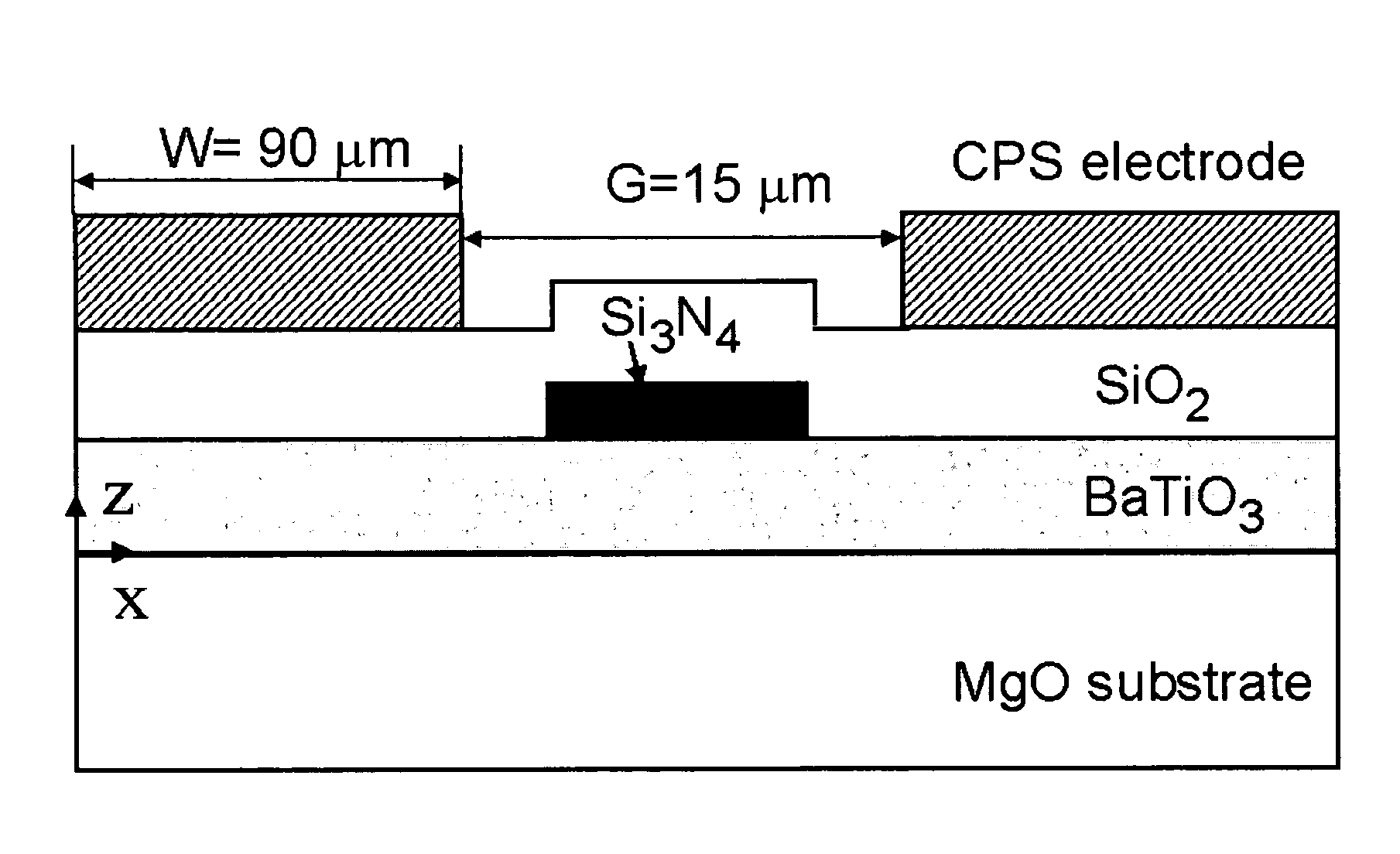
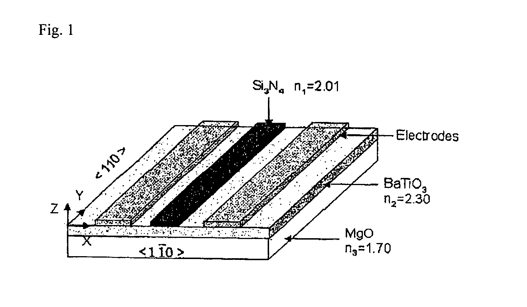
[0049]BaTiO3 thin films were deposited by low pressure MOCVD in a horizontal quartz reactor. The metal-organic precursors used were titanium tetraisopropoxide (TTIP, 99.999% purity) and a fluorinated barium precursor (Ba(hfa)2·PEB), prepared and purified as described in the literature. The oxidant was ultra-high purity oxygen. Argon was used as the carrier gas. Standard deposition conditions used source temperatures of 130° and 35° C. for Ba(hfa)2·PEB and TTIP, respectively. The oxygen flow rate of 100 sccm resulted in a partial pressure of 1.8 Torr, with a system pressure of ˜4 Torr. Carrier gas flow rates were 70 and 18 sccm for the Ba and Ti precursors. The TTIP line employed a 50 sccm dilutant flow between the bubbler and the reactor. The MgO (1 0 0) substrates were boiled in electronic grade acetone and methanol and ultrasonically cleaned prior to use.

example 2

[0050]The two-stage growth process included a low temperature nucleation stage (˜750° C.) and a high temperature growth stage (˜900° C.). After depositing for 5 min at 750° C., the temperature was rapidly ramped (˜2° / s) to high temperature with continuous film growth throughout the ramp process. Typical growth rates were 300–400 nm / h. The thickness of the nucleation layer is estimated at ˜20 nm, based on prism coupling measurements of a thick film grown under the low temperature conditions. Films from about 100 to about 1500 nm thick have been grown using this technique.

example 3

[0051]The phase purity, epitaxy, and crystallinity of the present films were examined using a four-circle X-ray diffractometer with a graphite monochromator and 12 kW rotating anode Cu Kα source. Film thickness and refractive index were measured using a Metricon 2010 prism coupler with a 632.8 nm laser source. A Digital Nanoscope III atomic force microscope (AFM) with Si3N4 tip was used to determine the root mean square (RMS) surface roughness and surface morphology. A Hitachi S4500 scanning electron microscope with cold field emission source was used for high resolution cross-sectional imaging.

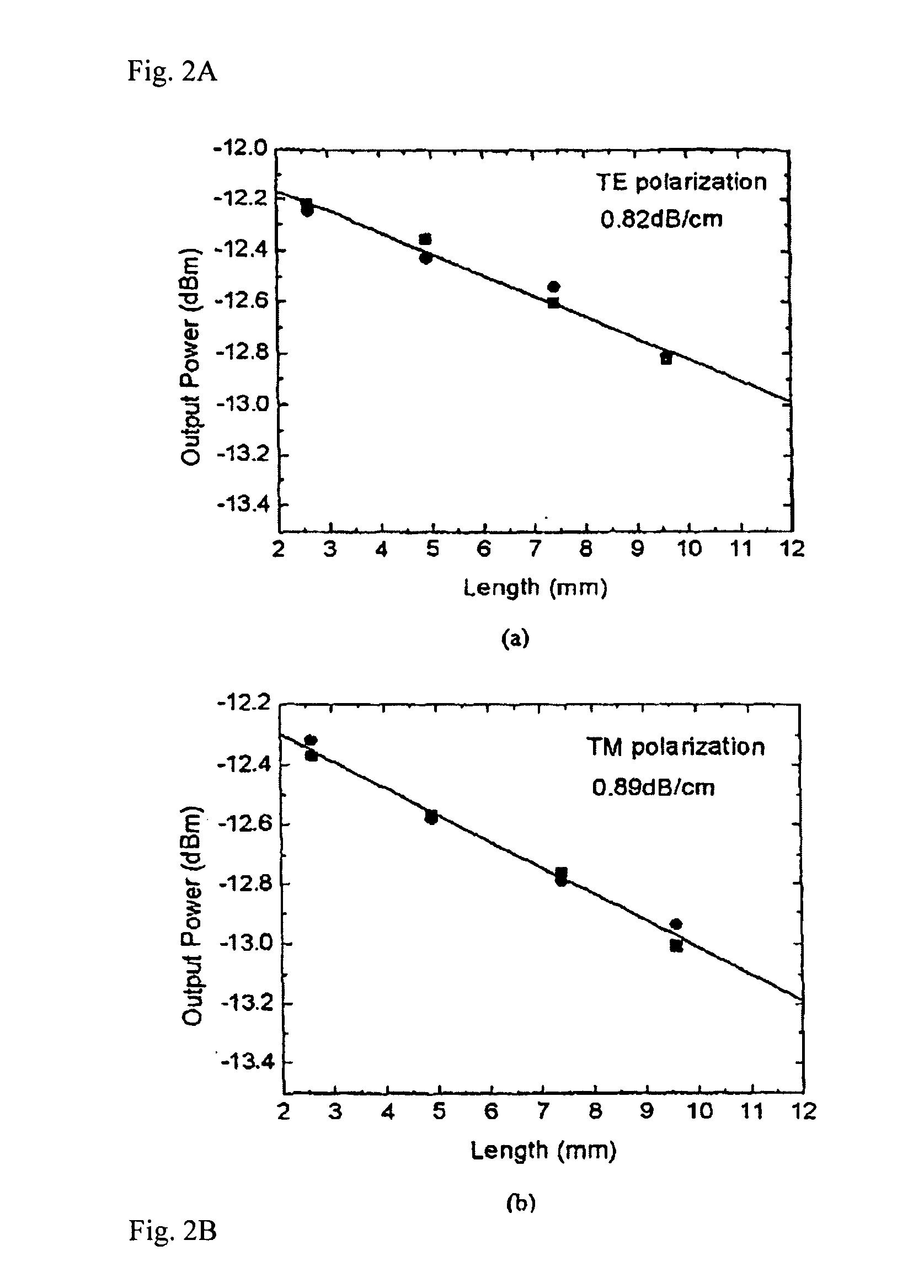
[0052]As demonstrated above, low loss, small size, low driving voltage waveguide modulator of this invention can be used as an optical building block for the next generation of ultra-broadband, high-speed fiber-optic Internet networks. Such a modulator can also be a key-enabling element for ultra-wideband optical signal processing applications, including large optical data handling in links o...


PUM

PropertyMeasurementUnit
thicknessaaaaaaaaaa
half-wave voltage lengthaaaaaaaaaa
wavelengthaaaaaaaaaa

Abstract

Electro-optic modulator devices and related waveguide components comprising BaTiO3 films.

Description

[0001]This application claims priority benefit from provisional application Ser. No. 60 / 627,252, filed Nov. 12, 2004, the entirety of which is incorporated herein by reference.[0002]The United States government has certain rights to this invention pursuant to Grant nos. F33615-02-C-5053 / P00001, P00002 and P00003 from the Department of Defense, and Grant nos. ECS-0123469 and DMR-0076977 from the National Science Foundation, all to Northwestern University.BACKGROUND OF THE INVENTION[0003]Electro-optic modulators are used for high-speed optical communication systems and ultrafast information processing applications. Bulk modulators of discrete electro-optic materials are possible, but typically with high driving voltage and narrow modulation bandwidth. To lower driving voltage and increase modulation bandwidth, materials with large electro-optic coefficients, low dielectric constants and single mode waveguide formation are required.[0004]The ferroelectric oxide, LiNbO3, has been widely...

Claims


Application Information

Patent Timeline
Patent Type & Authority Patents(United States)
IPC IPC(8): G02B6/10G02F1/035G02F1/295
CPCB82Y20/00G02F1/0356G02F2201/063G02F2201/066G02F2201/127G02F2202/36
Inventor WESSELS, BRUCE W.TANG, PINGSHENGTOWNER, DAVID J.MEIER, ANTHONY L.
Owner NORTHWESTERN UNIV
Why Eureka
Try Eureka