

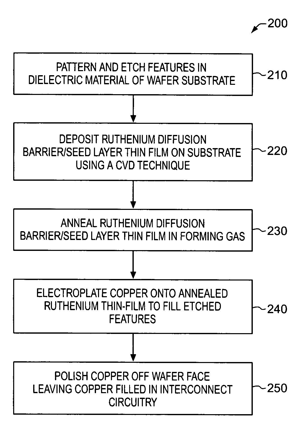
Anneal of ruthenium seed layer to improve copper plating
a seed layer and copper plating technology, applied in the field of metal plating, can solve the problems of ruthenium seed layer formation, poor morphology of thin film, and requirement of diffusion barrier layer, and achieve the effect of reducing oxides, reducing resistivity, and reducing terminal effects
- Summary
- Abstract
- Description
- Claims
- Application Information
AI Technical Summary
Benefits of technology
Problems solved by technology
Method used
Image

Examples
example 1
[0058]Adhesion tape tests were conducted to test the effect of ruthenium annealing in accordance with the invention on the adhesion between a ruthenium seed layer and copper that was electroplated onto the ruthenium seed layer.
[0059]Solid PDMAT (Pentakis dimethyl amidotantalum) was vaporized at 60° C. and about 0.5 Torr pressure into argon carrier gas flowing at 25 sccm. The PDMAT / argon gas stream was used to pretreat a series of 200 mm silicon semiconductor wafers having a substrate surface comprising PECVD silicon dioxide, SiO2. After PDMAT-pretreatment, a MOCVD technique was used to deposit a thin film of ruthenium metal, Ru, on each of several treated wafers. Each wafer was placed on a heated substrate holder in a CVD reaction chamber. The pressure of the chamber was maintained at about 7 Torr. The wafer was heated to a temperature of about 300° C. Solid dicyclopentadienyl ruthenium (RuCp2) was vaporized in a conventional gasification chamber at 120° C. into argon carrier gas. A...
example 2
[0065]The resistivity of ruthenium thin films before and after annealing of the thin films in accordance with the invention was measured.
[0066]Two 200 mm silicon semiconductor wafers having a substrate surface comprising PECVD silicon dioxide, SiO2, were pretreated as in Example 1. A ruthenium thin film was formed on each of the two 200 mm silicon semiconductor wafers using processes as described in Example 1. On one wafer, the resulting ruthenium thin-film had a thickness of approximately 4.0 nm. On the second wafer, the resulting ruthenium thin-film had a thickness of approximately 7.0 nm.
[0067]After storage in air exceeding seven days, the resistivity of each of the un-annealed ruthenium thin films was measured. Thereafter, each of the wafers containing a ruthenium thin film was treated by annealing in oxygen-free N2-gas (forming gas) in accordance with the invention at 400° C. for 90 seconds. Then, the resistivity of each of the annealed ruthenium thin films was measured. The re...
example 3
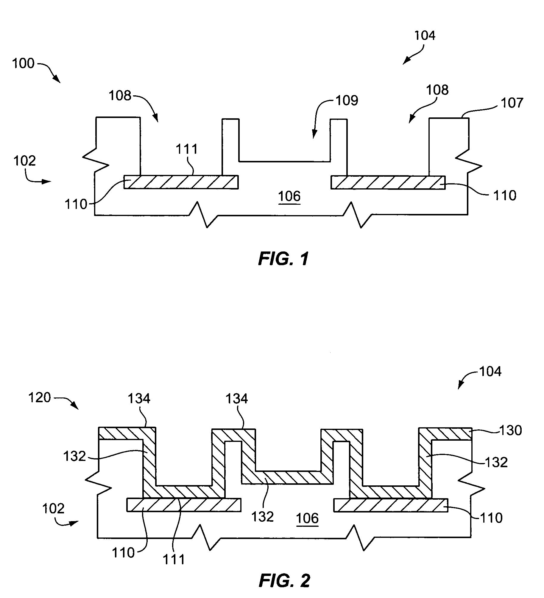
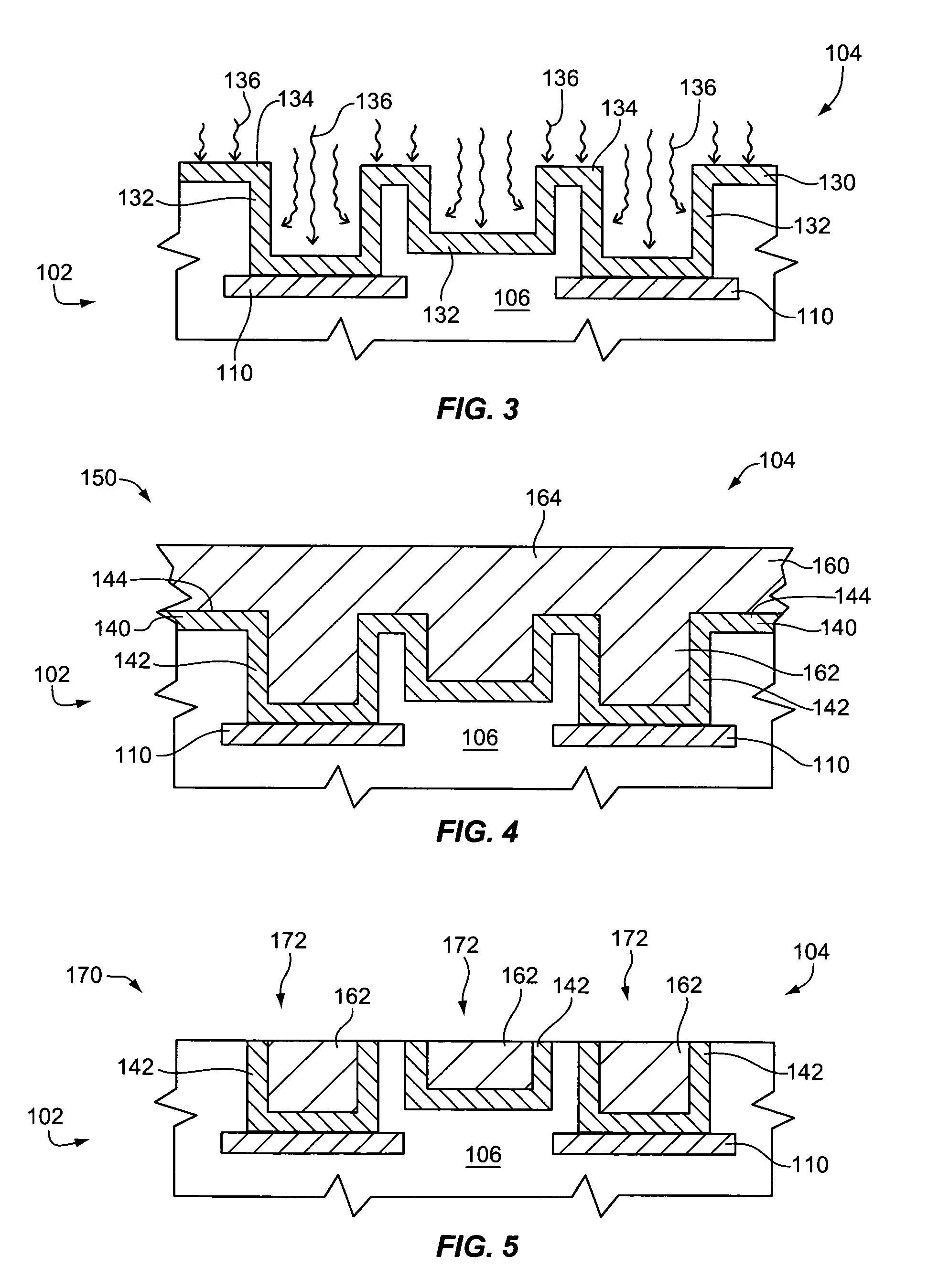
[0070]Two 200 mm silicon semiconductor wafers having a substrate surface comprising PECVD silicon dioxide, SiO2 were pretreated as in Example 1. FIGS. 7 and 8 depict schematically sections 300, 400 of semiconductor wafers 302, 402, respectively. As depicted in FIGS. 7 and 8, the wafers 302, 402 were patterned and etched using conventional techniques to form features in the SiO2 dielectric layer 306, 406. The etching processes formed exposed field surface 307, 407 of dielectric layer 306, 406. The etched features 308, 408 had shapes corresponding to circular vias having a diameter of 200 nm and a depth of 1100 nm. A ruthenium thin film was formed on each of the two 200 mm silicon semiconductor wafers using MOCVD processes as described in Example 1. Each of the resulting ruthenium thin films had a thickness of approximately 14 nm.
[0071]FIG. 7 depicts schematically ruthenium thin film 330 deposited on field surface 307 and on the inner surfaces of vias 308. Ruthenium thin film 330 was ...
PUM
| Property | Measurement | Unit |
|---|---|---|
| thickness | aaaaa | aaaaa |
| thickness | aaaaa | aaaaa |
| temperature | aaaaa | aaaaa |
Abstract
Description
Claims
Application Information