Remover compositions for dual damascene system

a damascene and composition technology, applied in the field of semiconductor device manufacture, can solve the problems of limiting device performance, interconnect rc delay time, and limiting device speed factor, so as to reduce the foaming effect, and inhibit corrosion.

Inactive Publication Date: 2009-06-16
EKC TECH
View PDF18 Cites 10 Cited by
  • Summary
  • Abstract
  • Description
  • Claims
  • Application Information

AI Technical Summary

Benefits of technology

[0088]XPS (X-Ray Photo Spectroscopy) analysis of such a structure shows the effect of the invention at removing CuO and CuO2 compounds (FIG. 4).
[0089]Table I summarizes various compositions used to clean such a structure, and their result on the cleaning efficiency and copper attack at the bottom of the structure. Results are rated from 0 to 10 by subjectively analyzing SEM pictures. A 0 rating means bad and 10 is good. However we note that if cleaning is bad, corrosion inhibition is usually good only because the residues protect the copper material. This is for example the case of pure water (A1).
[0090]From solutions A1, A2, A3, A4, and A5 we observe that cleaning efficiency increases when choline concentration reaches 20%. However we note that such concentration creates a thin foam at the surface of the solution and that adding a solvent such as, for example, propylene glycol, reduce this foaming effect without reducing the cleaning efficiency (solutions B1, B2, B3, B4, B5 and B6). This foaming effect however is reduced depending upon the type of stabilizer used with the raw material of choline hydroxide, and if the raw material is chosen correctly, the solution might not require an additional solvent.
[0091]We have investigated the process conditions for those cleaning solutions and found better results at temperatures below 50° C. The time does not appear to be important and we would recommend a process time between 10 and 30 minutes depending upon the difficulty of removing the residues.
[0092]Alternatively the use of other quaternary ammonium systems such as TMAH (Tetramethyl ammonium hydroxide), or TBAH (Tetrabutyl ammonium hydroxide) can have satisfactory results on the cleaning of such structures.
[0093]TABLE 1Result on Post Etch Residues cleaning and copperattack for various solutions (scored 0: bad to 10: good)Op.Op.CleaningCopperSolutionTemp.limeefficiencycorrosionA18015 010E78030 0 5E367010 710D21451010?10?D115010 710D125010 910D87010 9 5D104510 5 5D85010 5? 5D224515 710D2345152-510D2445150-210D254515 010D134515 710DI445150-2 5D154515 010D164515 9 9D174515 710D1845152-510B6501010 9A25010 7 2A35010 5 2A4501010 9A55010 910B1255 7 9B1755 9 9BI7525 710B2255 510B2755 510B275255-7 7B3255 010B3755 510B37525 510B42552-510B475252-510B5255 010B57557-910B575257-910B5501010 9B6255 910B6755 710B67525 710C65010 7 5C15010 7 9C25010 7 7C35010 7 5C450107-9 9C85010 7 5C95010 7 7C105010 510

Problems solved by technology

Since the introduction of 0.25 μm technology, interconnects are becoming the limiting speed factor of the device due to interconnect resistively as well as the RCA delay induced by adjacent interconnects.
A key challenge in reduced geometry devices, such as 0.18 μm technology, is the interconnect RC delay time, which becomes the limiting factor of the device performance.
However the main drawbacks of this material are (1) its high diffusivity into silicon, introducing risk of a “device-killing” defect in the front end device, and (2) the difficulty of dry etching copper containing metallurgies and integrating such metals in traditional processes.
Copper does not form an oxide passivation layer under ambient conditions (as aluminum does), making this metal very difficult to work with.
Accordingly, IC manufacturing requires the excellent cleaning of copper residues, as copper diffuses very easily into silicon dioxide and other dielectric materials ultimately risking the creation of a failure (“killing” the device) and effective removal of polymer and photoresist.
But the residues become more complex if the “opening” etch is done directly after the main etch or if the process does not use an etch stop layer and the opening etch is done simultaneously with opening the via—in a trench first dual damascene process.
Existing wet remover, stripping and cleaning compositions used in the semiconductor industry are not suitable in such situations for the following reasons:traditional amine-containing chemistries are not compatible with copper and dissolve the metal at the exposed areas;the variety of low-k and ultra low-k dielectrics used combined with continuing demands in performance and reductions of size (e.g., to nanometer ranges) requires a remover that has both broader range of application without a loss of effectiveness as a remover.acidic chemistries, such as dilute hydrofluoric acid solutions (DHF), have caused problems in unwantedly changing the designed dimentions of the device by aggressively attacking the sidewall of the dielectric.
Furthermore those solutions are ineffective for cleaning Cu2O or CFx compounds, typically found in back-sputtered residues and as contamination to dielectric materials and such chemistries do not effectively dissolve remaining polymers and photoresists, such as acrylate and methacrylate polymers transparent in lithography
Oxygen plasma ashing of remaining polymers and photoresists is not ideal in dual damascene processes and introduces additional problems, for example:an oxygen plasma step can oxidize exposed copper to the CuO and Cu2O states, which will increase the via resistance, andan oxygen plasma step can damage exposed organic dielectric material by etching the material in an uncontrolled manner, potentially compromising the integrity of the circuit.
It has been shown that a general trend to achieve lower dielectric constant uses less silicon and more carbon, often introducing voids.
Further, in certain dual damascene processes, e.g., via first, a crown or fence may be created on the top of the trench after the etch process which is difficult to remove.

Method used


Image

  • Remover compositions for dual damascene system
  • Remover compositions for dual damascene system
  • Remover compositions for dual damascene system

Examples


Embodiment Construction

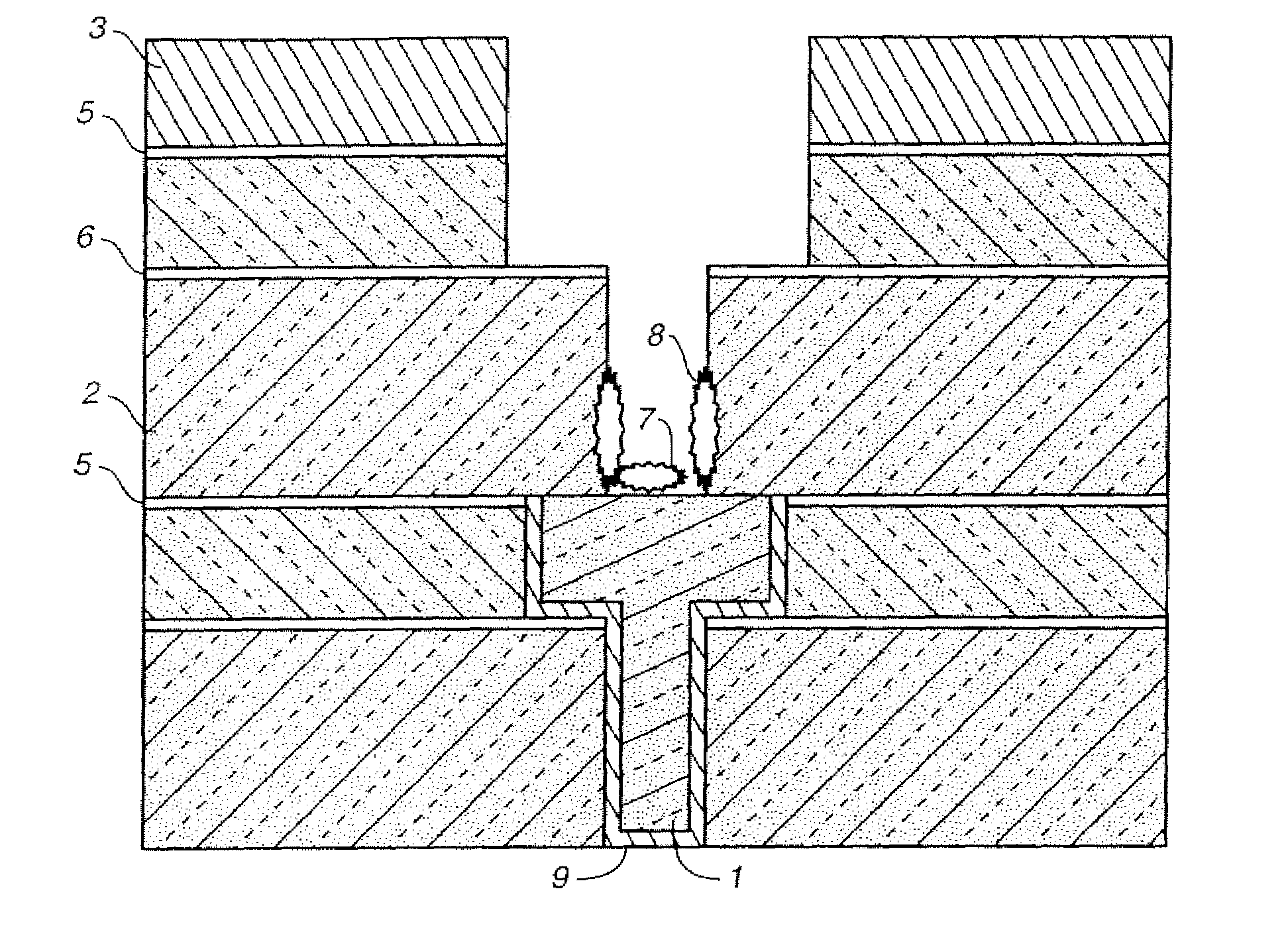
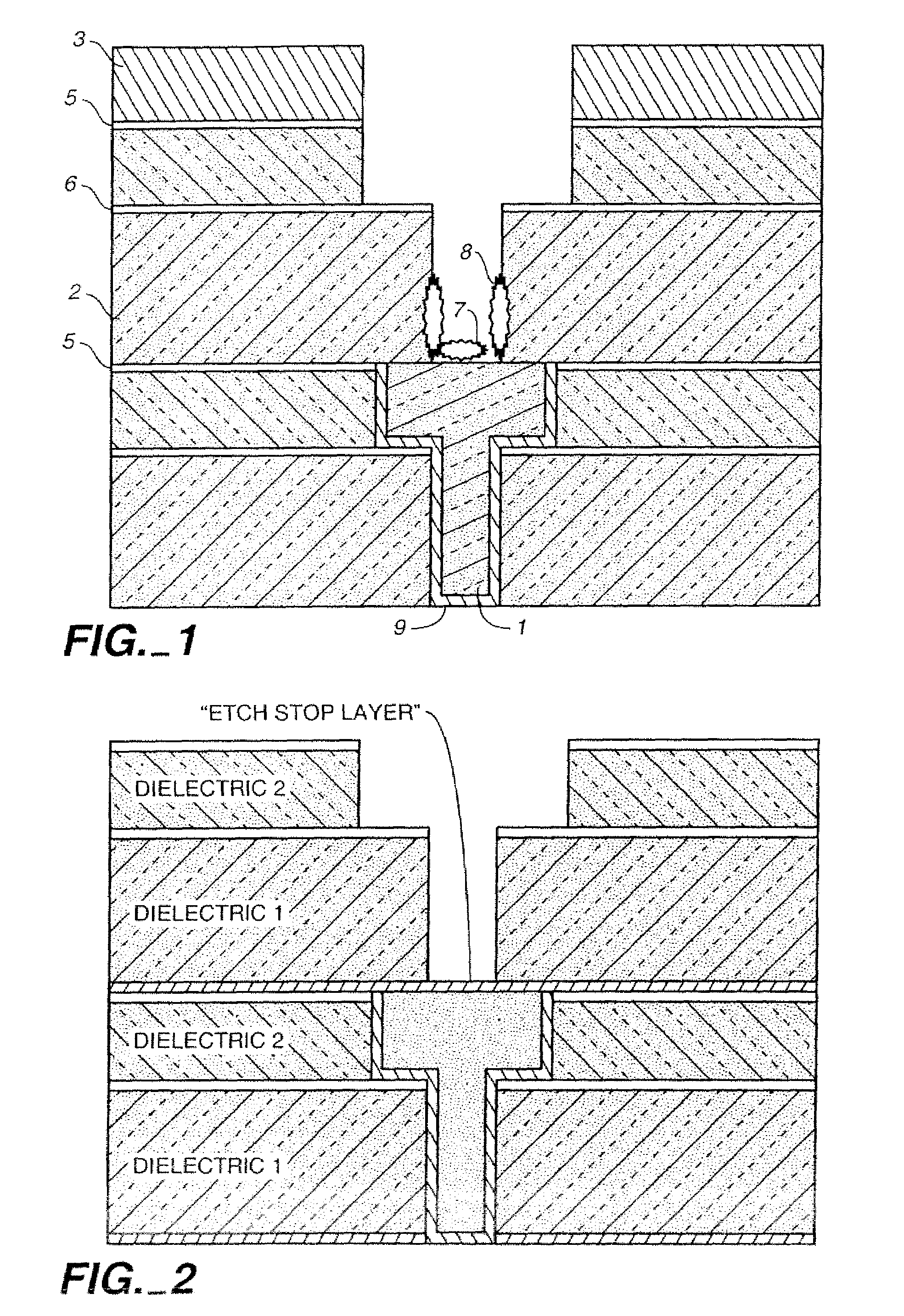
[0071]In the composition and process of this invention, the choline compound can be in the hydroxide or salt form, such as choline hydroxide, choline bicarbonate or choline chloride. As used herein, the term “choline compound” also embraces related quaternary ammonium compounds, such as tetramethylammonium hydroxide (TMAH), tetrabutyl ammonium hydroxide (TBAH), their salts, and the like.

[0072]Suitable organic solvents in the composition and for practice of the process include such polar solvents as dimethyl sulfoxide, ethylene glycol, ethylene glycol alkyl ether, diethylene glycol alkyl ether, triethylene glycol alkyl ether, propylene glycol, propylene glycol alkyl ether, N-substituted pyrrolidone, ethylene diamine and ethylene triamine. Additional polar solvents as known in the art can also be used in the composition of the present invention.

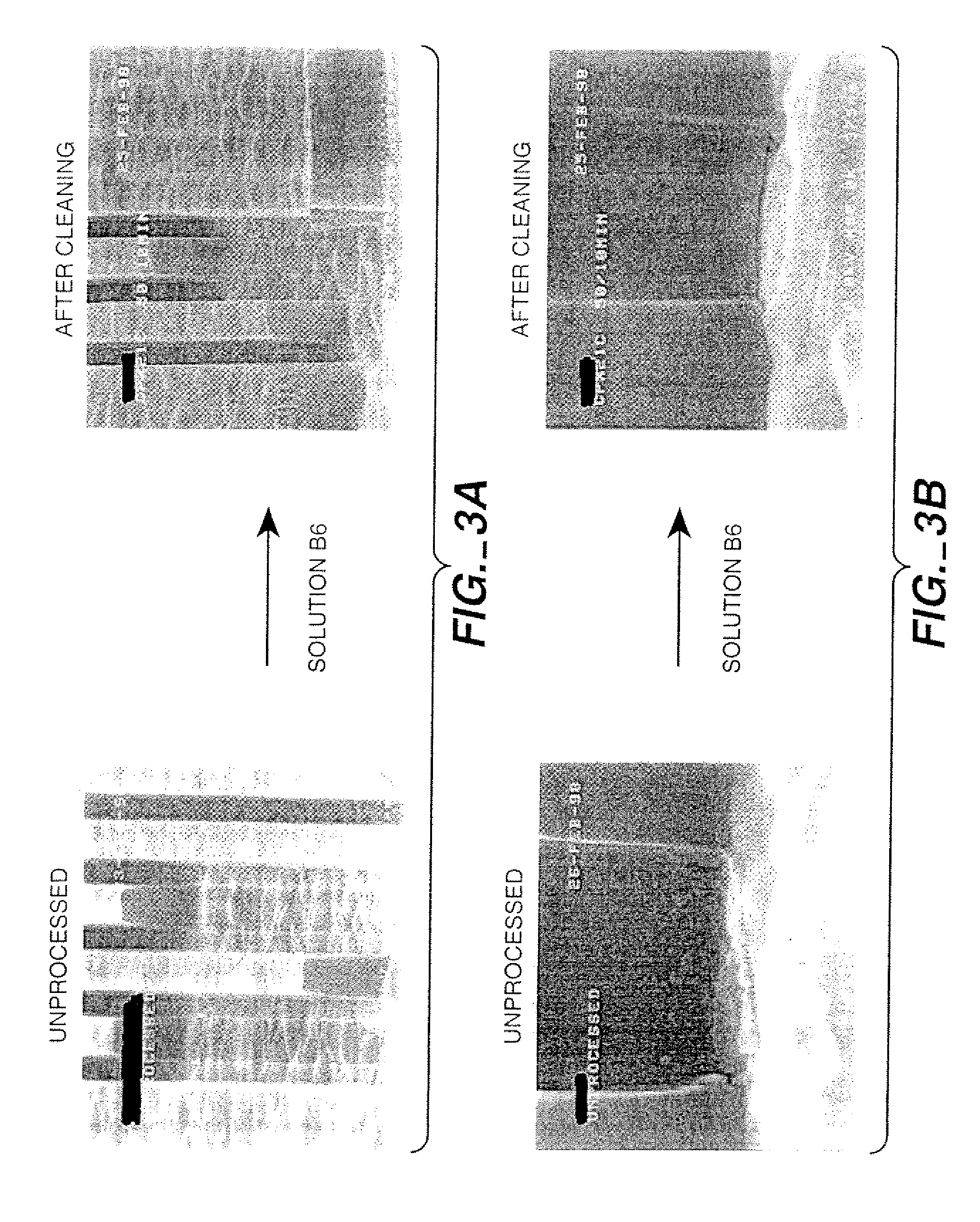
[0073]Optionally, a corrosion inhibitor may be included in a formulation used to clean damascene structures with exposed copper present. The c...


PUM

PropertyMeasurementUnit
feature sizesaaaaaaaaaa
temperaturesaaaaaaaaaa
dielectric constantaaaaaaaaaa

Abstract

A new remover chemistry based on a choline compound, such as choline hydroxide, is provided in order to address problems related to removal of residues, modified photoresists, photoresists, and polymers such as organic anti-reflective coatings and gap-fill and sacrificial polymers from surfaces involved in dual damascene structures without damaging the dielectrics and substrates involved therein. An etch stop inorganic layer at the bottom of a dual damascene structure may or may not be used to cover the underlying interconnect of copper. If not used, a process step of removing that protective layer can be avoided through a timed etch of the via in trench-first dual damascene processes.

Description

RELATED PATENT APPLICATIONS[0001]This is a continuation-in-part of U.S. patent application Ser. No. 10 / 689,657 filed Oct. 22, 2003 now U.S. Pat. No. 7,135,445, which is a continuation-in-part of U.S. application Ser. No. 10 / 007,134, filed Dec. 4, 2001 now U.S. Pat. No. 7,157,415, which is a divisional application of U.S. application Ser. No. 09 / 343,532, filed Jun. 30, 1999, now U.S. Pat. No. 6,417,112, which claims priority to U.S. Provisional Patent Application No. 60 / 092,024, filed Jul. 6, 1998, additionally claims priority to U.S. Provisional Patent Application No. 60 / 623,190, filed Oct. 29, 2004, and is related to a commonly-assigned, co-pending patent applications, entitled “Post Etch Cleaning and Stripping Compositions for Dual Damascene System,” filed on the same day as the instant application, the entire contents of which are each incorporated by reference herein.BACKGROUND OF THE INVENTION[0002]The present invention relates generally to manufacture of semiconductor devices ...

Claims


Application Information

Patent Timeline
Patent Type & Authority Patents(United States)
IPC IPC(8): C11D7/50C23F1/34C23G5/00G03F7/42H01L21/302H01L21/311H01L21/331H01L21/461H01L21/4763H05K3/26
CPCC23F1/34G03F7/423G03F7/425H01L21/02063H01L21/31133H05K3/26
Inventor LEE, WAI MUN
Owner EKC TECH
Why Eureka
Try Eureka