Semiconductor device and manufacturing method thereof

a semiconductor and semiconductor technology, applied in the field of semiconductor devices, can solve the problems of increasing the mounting cost of silicon chips, the inability to adapt to the shape of the curved surface of the article, and the inability to reduce the unit cost of wireless chips, so as to reduce the plane area of the driver circuit of the memory, the effect of reducing the unit cost of the chip and reducing the voltage value of the signal obtained by the antenna

Inactive Publication Date: 2010-05-11
SEMICON ENERGY LAB CO LTD
View PDF52 Cites 23 Cited by
  • Summary
  • Abstract
  • Description
  • Claims
  • Application Information

AI Technical Summary

Benefits of technology

[0011]A conventional wireless chip is manufactured using an expensive silicon wafer similarly to a microprocessor or semiconductor memory. Therefore, there has been an inevitable limit to reduce unit cost of the wireless chip. In particular, a memory region which is needed for the wireless chip occupies a large area in a silicon chip, and it has been necessary to reduce the area occupied by the memory region without changing memory capacity for reducing the unit cost of the chip. In addition, although reduction in cost can be expected by reduction in the size of the silicon chip, if reduction in the size of the silicon chip proceeds, mounting cost of the silicon chip is increased. In order to distribute the chip to the market, it is very important to reduce the unit cost of the chip, which is one of priorities in commodity production.

Problems solved by technology

Therefore, there has been an inevitable limit to reduce unit cost of the wireless chip.
In addition, although reduction in cost can be expected by reduction in the size of the silicon chip, if reduction in the size of the silicon chip proceeds, mounting cost of the silicon chip is increased.
In addition, the conventional wireless chip is not suitable for being attached to a curved surface of an article even if it is a smaller piece because it uses silicon for a structure.
Although there has been a method of grinding and polishing a silicon wafer itself to thin the silicon wafer, the number of steps is increased due to the step, and thus, it has been contradictory to reduction in manufacturing cost.
Even if a wireless chip is thinned, in the case of an IC tag which is attached to an article to be used, when the wireless chip is attached to a thin substrate (e.g., strip of film or slip of paper), disfigurement is caused because a protrusion is generated on a surface of the substrate.
In addition, since a protrusion is generated on the surface of the substrate, in the case of performing printing to a substrate such as slip of paper, high-definition printing becomes difficult.
Furthermore, when a silicon chip has been thinned, mechanical strength of the silicon chip could have been decreased and the silicon chip could have been broken when a substrate is bent.
Each silicon chip is minute, and a manufacturing device for supplying current for writing different information to ROM formed in each silicon chip needs precision location alignment or the like, thereby being expensive.
Therefore, manufacturing cost is increased due to this manufacturing device.

Method used


Image

  • Semiconductor device and manufacturing method thereof
  • Semiconductor device and manufacturing method thereof
  • Semiconductor device and manufacturing method thereof

Examples


embodiment 1

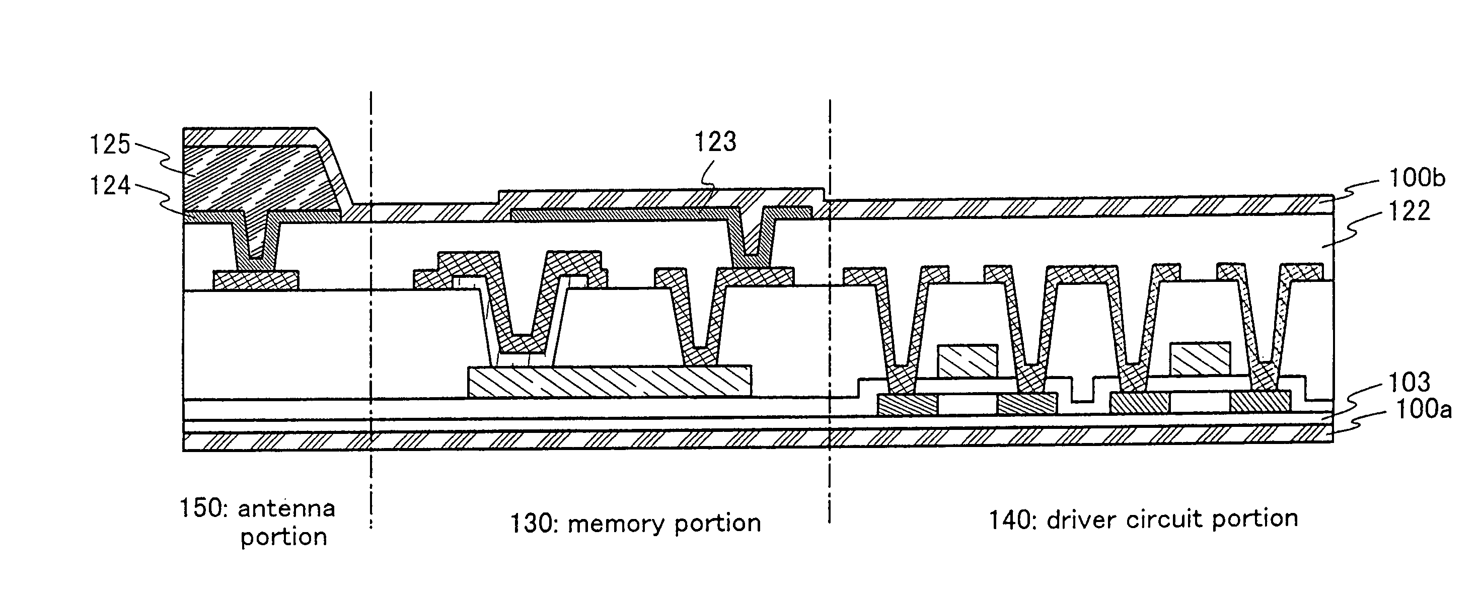
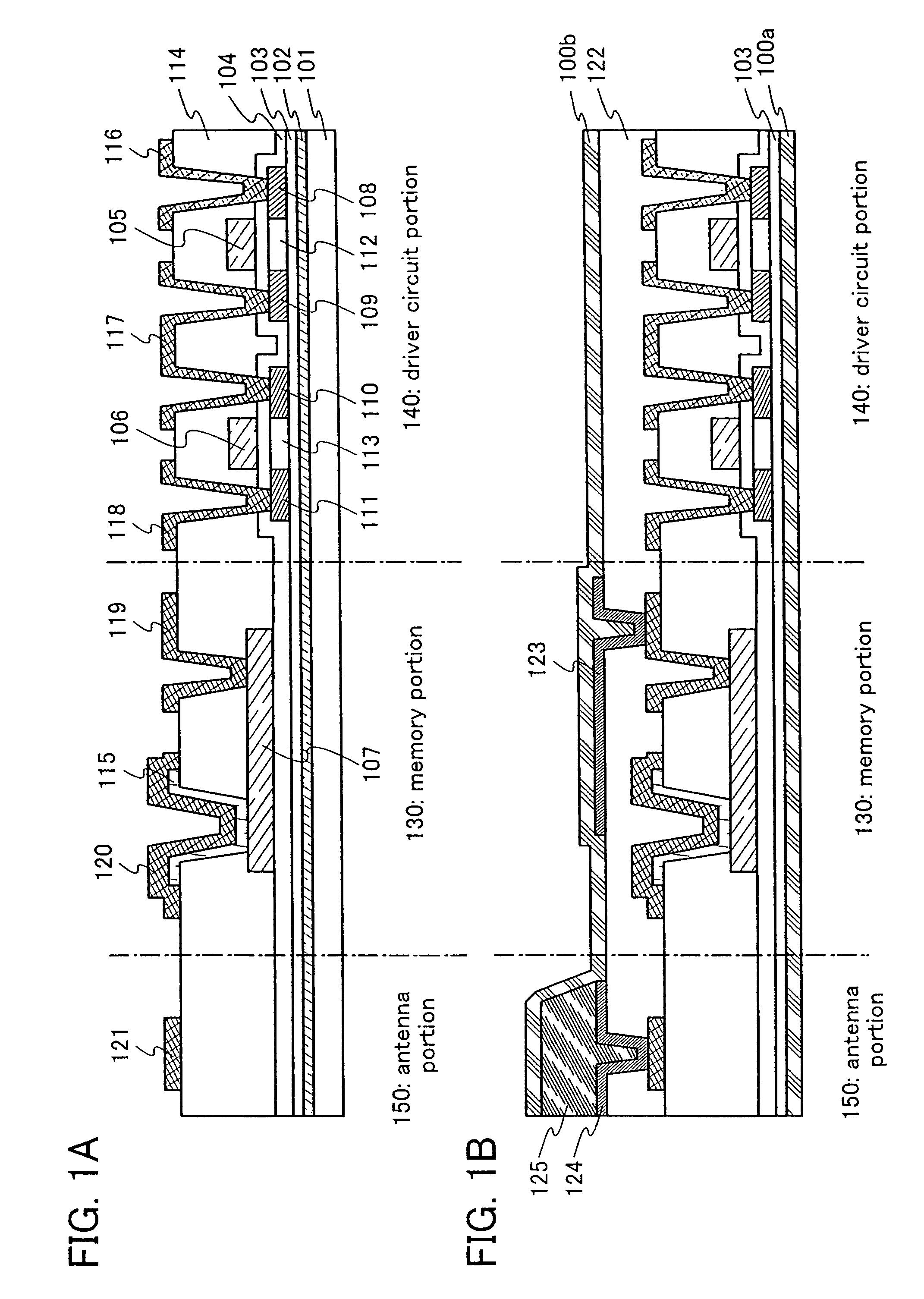
[0098]In this embodiment, a manufacturing method of a wireless chip including active matrix antifuse-type ROM will be explained below with reference to FIGS. 8A to 8D and FIGS. 9A to 9C.

[0099]First, a metal layer 502 which serves as a peeling layer is formed over a substrate 501. A glass substrate is used as the substrate 501. A tungsten film, a tungsten nitride film, or a molybdenum film with a thickness of 30 to 200 nm which is obtained by a sputtering method is used for the metal layer 502.

[0100]Next, a surface of the metal layer 502 is oxidized to form a metal oxide layer (not shown). The metal oxide layer may be formed by oxidation of the surface with pure water or ozone water or oxidation with oxygen plasma. Alternatively, the metal oxide layer may be formed by heating in an atmosphere containing oxygen. Further alternatively, the metal oxide layer may be formed in a later step of forming an insulating film. In this case, when a silicon oxide film or a silicon oxynitride film ...

embodiment 2

[0140]In this embodiment, an example in which a process is partly different from that of Embodiment 1 will be shown in FIGS. 10A to 10D and FIGS. 11A to 11C. Note that portions which are common to those in Embodiment 1 are denoted by the same reference numerals, and the same explanation is omitted for simplification.

[0141]First, the same cross-sectional structure as FIG. 8A is obtained according to Embodiment 1. Note that FIG. 10A is the same as FIG. 8A.

[0142]Next, a silicon film is formed by a sputtering method, an LPCVD method, a plasma CVD method, or the like, and a metal film is stacked thereover by a sputtering method or a plasma CVD method. Any one of an amorphous silicon film, a microcrystalline silicon film, and a polysilicon film is used as the silicon film. A thickness of the silicon film is 10 to 200 nm. The metal film is formed using a simple substance such as titanium, tungsten, nickel, chromium, molybdenum, tantalum, cobalt, zirconium, vanadium, palladium, hafnium, pla...

embodiment 3

[0162]A semiconductor device of this embodiment will be explained with reference to FIG. 12. As shown in FIG. 12, a semiconductor device 1520 of the present invention has a function of performing noncontact data communication. The semiconductor device 1520 includes a power supply circuit 1511, a clock generation circuit 1512, a data demodulation / modulation circuit 1513, a control circuit 1514 which controls other circuits, an interface circuit 1515, a memory circuit 1516, a data bus 1517, an antenna 1518, a sensor 1523a, and a sensor circuit 1523b. In FIG. 12, a driver circuit refers to the power supply circuit 1511, the clock generation circuit 1512, the data demodulation / modulation circuit 1513, the control circuit 1514 which controls other circuits, and the interface circuit 1515.

[0163]The power supply circuit 1511 generates various power supply voltage to be supplied to each circuit in the semiconductor device 1520, based on an AC signal inputted from the antenna 1518. The clock...


PUM


Abstract

An object is to provide a semiconductor device mounted with memory which can be driven in the ranges of a current value and a voltage value which can be generated from a wireless signal. Another object is to provide write-once read-many memory to which data can be written anytime after manufacture of a semiconductor device. An antenna, antifuse-type ROM, and a driver circuit are formed over an insulating substrate. Of a pair of electrodes included in the antifuse-type ROM, the other of the pair of the electrodes is also formed through the same step and of the same material as a source electrode and a drain electrode of a transistor included in the driver circuit.

Description

TECHNICAL FIELD[0001]The present invention relates to a semiconductor device having a circuit including a thin film transistor (hereinafter, referred to as a TFT) and a manufacturing method thereof. For example, the present invention relates to an electronic appliance in which an electro-optical device typified by a liquid crystal display panel or a light-emitting display device including an organic light-emitting element is mounted as a component.[0002]Note that a semiconductor device in this specification refers to a general device which can function by utilizing semiconductor characteristics, and an electro-optical device, a semiconductor circuit, and an electronic appliance are all semiconductor devices.BACKGROUND ART[0003]Various types of memory have conventionally been proposed. As typical memory, the following can be given: memory including an electromagnetic tape or an electromagnetic disk, RAM capable of writing and reading, ROM only for reading (read only memory), and the ...

Claims


Application Information

Patent Timeline
Patent Type & Authority Patents(United States)
IPC IPC(8): H01L29/786
CPCG11C17/16H01L27/105H01L27/11206H01L27/1255H01L27/11286H01L23/5252H01L2924/0002H01L2924/00H10B20/20H10B20/60H01L27/1214H01L27/13H01L29/458
Inventor TOKUNAGA, HAJIME
Owner SEMICON ENERGY LAB CO LTD
Why Eureka
Try Eureka