Method and apparatus for forming device quality gallium nitride layers on silicon substrates

a technology of gallium nitride and thin film, which is applied in the direction of polycrystalline material growth, chemically reactive gas growth, crystal growth process, etc., can solve the problems of silicon devices that silicon devices have significant limitations in power applications, and silicon devices have failed to provide the desired electrical properties in many applications. , to achieve the effect of improving the crystal lattice structur

Inactive Publication Date: 2018-05-01
VEECO INSTR
View PDF6 Cites 1 Cited by
  • Summary
  • Abstract
  • Description
  • Claims
  • Application Information

AI Technical Summary

Benefits of technology

[0023]The present invention addresses the problems of the prior art described above by providing a deposition process that operates at considerably lower reaction temperatures as compared to conventional high-temperature deposition processes such chemical vapor deposition (CVD) to avoid the problems of wafer bowing and device layer cracking associated with high temperature heteroepitaxial growth and further allows application of thicker device layers normally prohibited by high temperature heteroepitaxial growth processes which suffer from increased wafer bow and device layer cracking in proportion to the device layer thickness. In particular the present invention utilizes atomic layer deposition (ALD) to deposit group III-V and group II-VI compounds and group III-N compounds directly onto a substantially single crystal silicon substrate surface, e.g. the Si (111) plane using an Atomic Layer Deposition (ALD) film deposition process at a low reaction temperature, e.g. less than 800° C. and preferably less than 400° C., and thereafter thermally annealing the film layer in a manner that causes improvements in the crystal lattice structure to the extent that the improved crystal lattice structure of the deposition film exhibits a lattice structure that is more characteristic of a single crystal lattice structure as determined by X-RAY Diffraction (XRD) analysis. In addition, the present invention utilizes Domain Matching Epitaxy (DME) to at interfaces between dissimilar materials to further alleviate problems associated with crystal lattice spacing mismatches associated with heteroepitaxial growth.

Problems solved by technology

In practice flaws in the single crystal structure potentially leading to cracking in the device layer especially when the device layer is stressed by a rapid thermal cycling.
However, silicon devices have failed to provide the desired electrical properties in many applications, especially in power devices such as power switches and rectifiers and further in optical devices that benefit from higher band gap materials such a Gallium Nitride (GaN).
In particular, silicon has significant limitations in power applications particularly with respect to excessive Joule heating which consumes operating power and is largely the reason why electronic systems require cooling, which further consumes operating power.
This is especially problematic in battery powered systems where battery powered operating time is significantly reduced by Joule heating and system cooling used to alleviate the Joule heating.
Another silicon based device limitation in power devices is its relatively low blocking voltage which limits the use of many silicon devices to low voltage applications, (e.g. <200 volts).
A further silicon based device limitation is its relatively low bandwidth which limits switching speed in high speed devices such as switching power supplies of DC-DC power converters and limits its optical properties for use in visible wavelength emitters.
However, in both of these solutions the need for a non-silicon substrate layer requires specialized processing equipment to grow and process non-silicon substrates substantially increasing end user device cost and virtually eliminates integration of GaN devices into silicon based integrated circuits except as an added stand-alone component.
While these conventional solutions meet a niche demand for GaN devices where a silicon device is inadequate; they come at a high cost and in limited configurations mainly due to their inability to be manufactured using convention silicon based processes.
While it is widely accepted that the high reaction temperature of the MOCVD process favors heteroepitaxial growth that exhibits single crystal film behavior e.g. as determined by X-ray diffraction analysis, the high reaction temperature has other drawbacks associated with stresses induced into the substrate and the device layer as a result of rapid and often non-homogeneous heating and cooling during the deposition process as well as the incorporation of unwanted materials into the substrate, e.g. caused by diffusion of the device layer material into the substrate.
In a conventional MOCVD reactor, stress management is a primary concern and limits the quality of the deposition.
While this problem has been addressed by forming “stress compensation layers” in MOCVD films these stress compensation layers degrade the device layer performance and add cost.
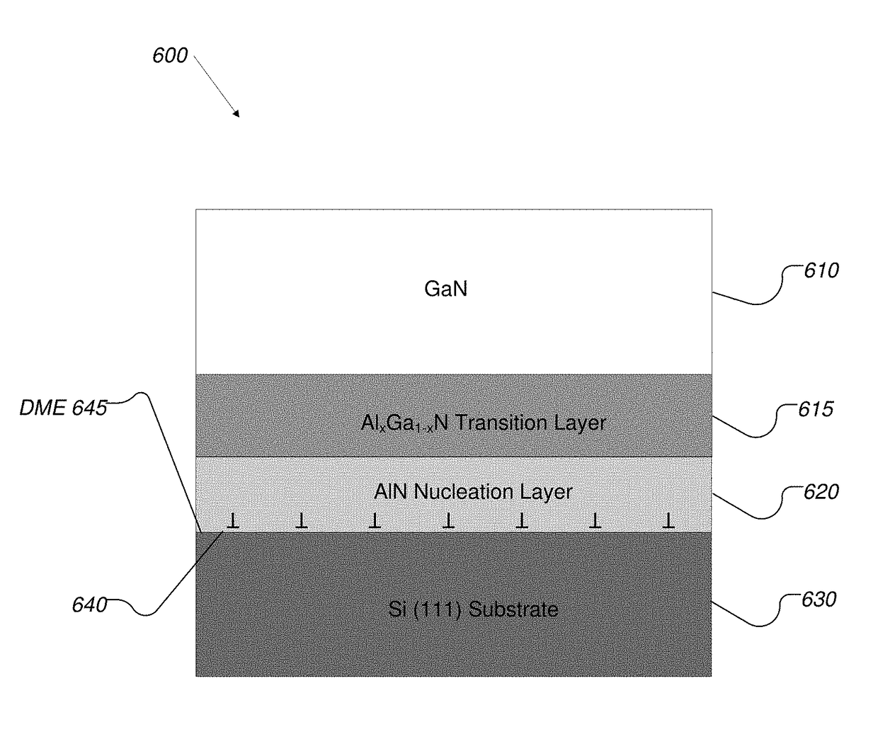
However when the GaN is grown directly onto the silicon substrate there is undesirable cracking due to the large 
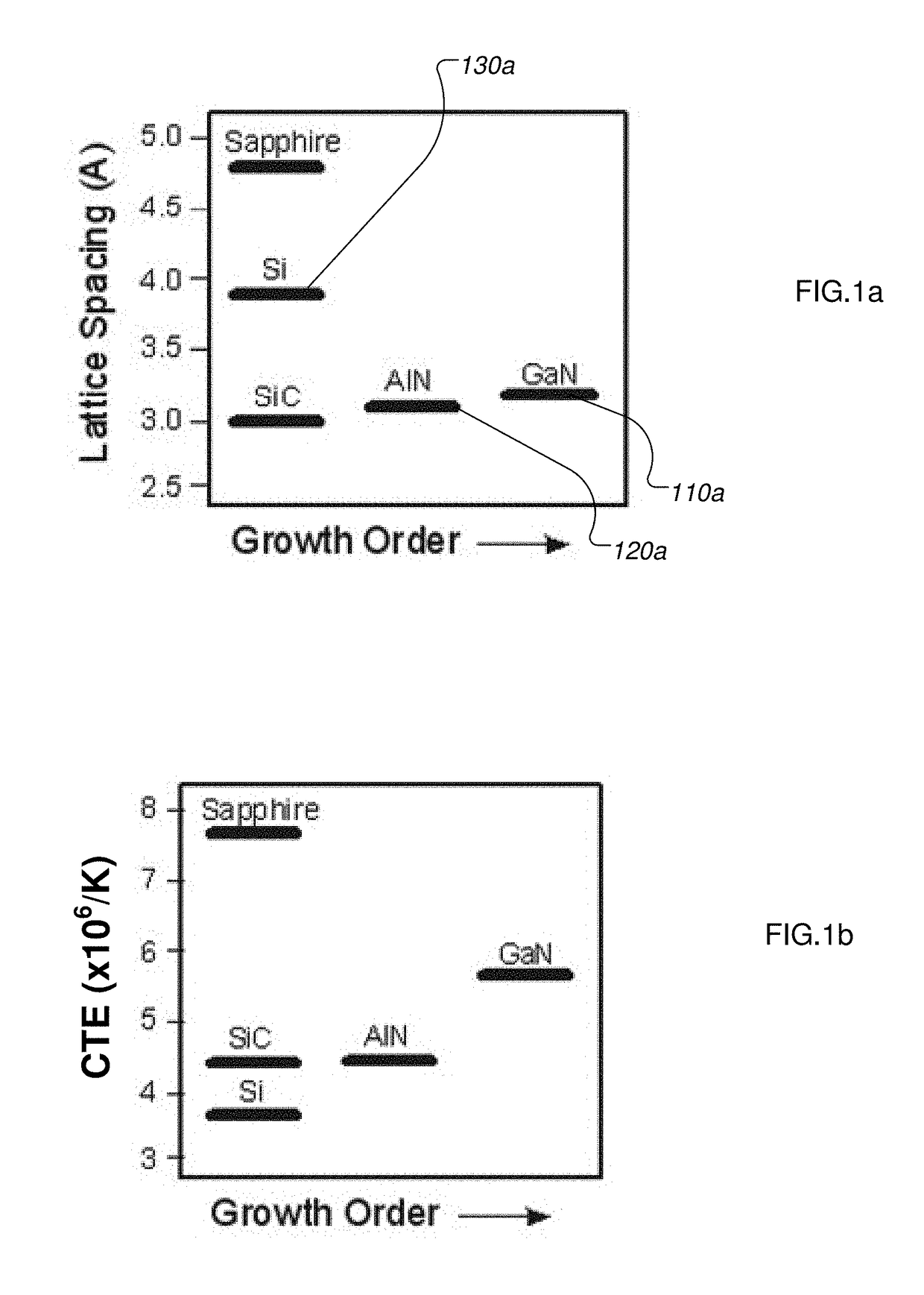
crystal lattice spacing mismatch (16.9%) between the GaN and the silicon and the large coefficient of thermal expansion (CTE) mismatch between GaN (αa 5.59×10⁻⁶ K−1) and Si(αa 3.77×10⁻⁶ K−1).
The problem is that the nucleation layer is polycrystalline due to the crystal lattice spacing mismatch between AlN and Si, and the spacing mismatch causes the grain boundaries between the nucleation layer and the GaN layer to produce a high density of dislocations or domain mismatches in the epitaxial GaN layer.
While Pan et al. report that cracking in the GaN layer is reduced by the application of the high temperature H-T AlN buffer or nucleation layer which provides less lattice spacing mismatch with the GaN layer as compared to the lattice spacing mismatch of GaN with the silicon substrate: this solution fails to address the problems associated with high reaction temperature of the MOCVD process which still leads to wafer bow, which increases with increased device layer thickness.
Accordingly, no solution is currently provided to overcome the need for high temperature epitaxial growth provided by MOCVD and other high temperature deposition techniques while avoiding the problems associated with the resulting wafer bow and cracking typical of high reaction temperature processes.
Finally, there is a further important limitation imposed by the approach of growing GaN on a dissimilar substrate with a nucleation layer.
In particular, the key role of the nucleation layer in promoting the epitaxial growth precludes the option of having device layers at the bottom of the GaN film for vertical device architectures.
Unfortunately, this limitation is devastating for designing high-power devices, where the vertical architectures often have significant performance advantages in carrying high current loads and blocking high voltage.
Accordingly, no solution is currently provided to overcome the need for building vertical devices when the device layer includes a nucleation layer applied between the substrate and the device layer.
All three of these applications require the fabrication of high quality (low defect) GaN films which is are not adequately addressed in the art.

Method used


Image

  • Method and apparatus for forming device quality gallium nitride layers on silicon substrates
  • Method and apparatus for forming device quality gallium nitride layers on silicon substrates
  • Method and apparatus for forming device quality gallium nitride layers on silicon substrates

Examples


Embodiment Construction

5.1 Exemplary System Architecture

[0040]According to one aspect of the present invention Atomic Layer Deposition (ALD) is used to deposit thin films onto planar and non-planar silicon substrate surfaces in processes related to the manufacture of solid state electronic devices. According to one aspect of the present invention ALD deposition film growth or film deposition described herein is preferably conducted at reaction temperatures ranging from 80-400° C. wherein substrates are housed in a reaction chamber and maintained below atmospheric pressure e.g. at a pressure ranging from 1-500 mTorr (milli-torr) during the film deposition process. Notwithstanding the desirability to limit ALD reaction temperatures to the preferred range of 80-400° C., ALD reaction temperatures ranging from 80-800° C. may be used without deviating from the present invention. Specifically, the reaction temperature means the temperature of the substrate being deposition coated and the temperature of the depos...


PUM

PropertyMeasurementUnit
reaction temperatureaaaaaaaaaa

Abstract

Atomic Layer Deposition (ALD) is used for heteroepitaxial film growth at reaction temperatures ranging from 80-400° C. The substrate and film materials are preferably matched to take advantage of Domain Matched Epitaxy (DME). A laser annealing system is used to thermally anneal deposition layer after deposition by ALD. In preferred embodiments, a silicon substrate is overlaid with an AlN nucleation layer and laser annealed. Thereafter a GaN device layer is applied over the AlN layer by an ALD process and then laser annealed. In a further example embodiment, a transition layer is applied between the GaN device layer and the AlN nucleation layer. The transition layer comprises one or more different transition material layers each comprising a AlxGa1-xN compound wherein the composition of the transition layer is continuously varied from AlN to GaN.

Description

1 CROSS REFERENCE TO RELATED U.S. PATENT APPLICATIONS[0001]This application is a continuation of U.S. patent application Ser. No. 14 / 909,004 which is a 371 entry of PCT Appl. No. PCT / US14 / 56172 on Sep. 17, 2014 which claims the benefit of U.S. Provisional Appl. No. 61 / 881,369 filed Sep. 23, 2013 entitled DEPOSITION AND PROCESSING METHODS FOR GROWING GALLIUM NITRIDE AND ALUMINUM NITRIDE ON SILICON both of which are incorporated herein in their entireties.2 BACKGROUND OF THE INVENTION2.1 Field of the Invention[0002]The exemplary, illustrative, technology herein relates to systems and methods for growing device quality Gallium Nitride (GaN) thin film layers onto a silicon substrate.[0003]The technology herein has applications in the areas of solid state power devices such as switches; rectifiers and other power devices as well as electro-optical devices such as lasers and light emitting diodes (LEDs) whether fabricated as a stand-alone device or incorporated into a solid state integrat...

Claims


Application Information

Patent Timeline
Patent Type & Authority Patents(United States)
IPC IPC(8): H01L29/15H01L29/20H01L21/324C30B29/06C30B29/40C30B25/18H01L31/0256H01L21/02
CPCH01L21/0251C30B25/183C30B29/06C30B29/406H01L21/0254H01L29/2003H01L21/02381H01L21/02433H01L21/02458H01L21/02694H01L21/3245H01L21/0262C30B25/02C23C16/303C30B29/403C23C16/45527C23C16/45536C23C16/46C23C16/56
Inventor SUNDARAM, GANESHHAWRYLUK, ANDREW M.STEARNS, DANIEL
Owner VEECO INSTR
Why Eureka
Try Eureka