Silicon substrate top emission organic light emitting microdisplay and method for producing same

A technology of microdisplay and organic light-emitting layer, which is applied in static indicators, semiconductor/solid-state device manufacturing, instruments, etc., can solve the problems of not pointing out the structure and manufacturing process of silicon-based microdisplays, and easily introducing pollution and pollution.

Active Publication Date: 2012-08-08
LUMICORE MICROELECTRONICS SHANGHAI CO LTD
View PDF7 Cites 34 Cited by
  • Summary
  • Abstract
  • Description
  • Claims
  • Application Information

AI Technical Summary

Problems solved by technology

[0004] Chinese patent 101447509 and Chinese patent 101459226 disclose a production method of a top-emitting organic display and its anode structure, but this method requires secondary processing of the organic light-emitting anode material after taking out the wafer from the CMOS foundry. Switching between different processes is easy to introduce pollution. On the other hand, it is necessary to build a new dedicated production line with an investment of over 100 million
Chinese patent 101393891A discloses a method for preparing a silver electrode on the sur

Method used


Image

  • Silicon substrate top emission organic light emitting microdisplay and method for producing same
  • Silicon substrate top emission organic light emitting microdisplay and method for producing same
  • Silicon substrate top emission organic light emitting microdisplay and method for producing same

Examples


Embodiment 1

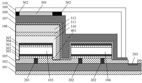
[0057] see figure 1 , the silicon-based top-emitting organic light-emitting microdisplay: the organic light-emitting device is fabricated on the surface of the silicon-based chip, the driving circuit and the control circuit of the organic light-emitting device are integrated in the silicon-based chip, and the light source generated by the organic light-emitting device passes through the top of the microdisplay Issued externally, its structure includes:

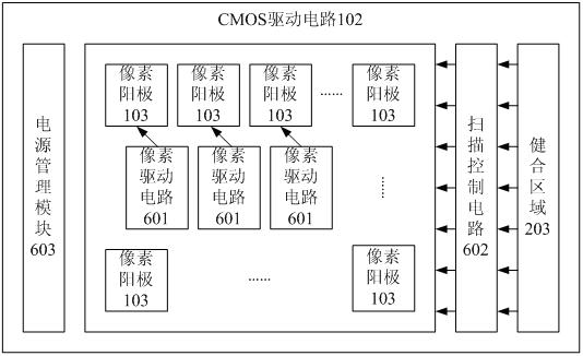
[0058] (1) A single crystal silicon substrate 101 and a driving circuit layer 102;

[0059] (2) a top via layer 105 for generating vias;

[0060] (3) organic light-emitting pixel anodes 103 arranged in an array, and the pixel anodes 103 have a vertical five-layer dielectric structure;

[0061] (4) One or more organic light-emitting common cathode electrodes 104;

[0062] (5) The via hole 201 located under the pixel anode 103 and the via hole array 202 located under the common cathode electrode 104;

[0063] (6) Bonding are...

Embodiment 2

[0071] This embodiment is basically the same as Embodiment 1, and the special features are as follows:

[0072] The current path of organic luminescence is: external power supply -> positive power supply pin of bonding area 203 -> driving circuit layer 102 -> through hole 201 -> pixel anode 103 -> organic layer 106 -> transparent cathode layer 107 -> total Cathode electrode 104 -> through hole array 202 -> driving circuit layer 102 -> negative power supply pin of bonding area 203 -> external power supply. The current flowing through a single anode pixel does not exceed 80 nanoamps.

[0073] The driving circuit layer 102 is manufactured using a CMOS integrated circuit process, and its transistor feature size is 0.6 micron, 0.5 micron, 0.35 micron, 0.25 micron, 0.18 micron, 0.13 micron or other typical deep submicron process size, and supports dual voltage or multi-voltage In the region, the analog circuit voltage range is -5V to +5V, and the digital circuit voltage range is +1...

Embodiment 3

[0095] The process flow of the silicon-based top-emitting organic light-emitting microdisplay preparation method is as follows:

[0096] (1) Manufacture the driving circuit 102 on the single crystal silicon substrate 101 according to the CMOS process.

[0097] (2) Using the mask plate of the via layer, the top via layer 105 , the via holes 201 and the via hole array 202 are manufactured by chemical vapor deposition.

[0098] (3) Make the pixel anode 103 and the common cathode electrode 104 using the top metal layer mask. This process includes cleaning, dehydration, coating, glue coating, photolithography, development, etching, and glue removal. The coating process includes physical vapor phase deposition and chemical vapor deposition.

[0099] (5) Using a bonding layer mask, etch the top via layer to form a bonding region 203 .

[0100] (6) Cutting the wafer to form a micro-display silicon-based chip.

[0101] (7) Using an organic layer mask and a vacuum evaporation process...


PUM

PropertyMeasurementUnit
Thicknessaaaaaaaaaa
Thicknessaaaaaaaaaa
Unit areaaaaaaaaaaa

Abstract

The invention relates to a silicon substrate top emission organic light emitting microdisplay and method for producing the same. An organic light emitting device is arranged on the surface of a silicon-based chip, and a driving circuit and a controlling circuit of the organic light emitting device are integrated in the silicon-based chip. The structure (from bottom to top) of the microdisplay is a monocrystalline silicon substrate, the driving circuit, a top through-hole layer and a top through-hole, a pixel anode and a common-cathode, an organic layer, a transparent cathode layer, a multi-layer film packaging layer, a color filtering layer and a glass sealing cap, wherein the pixel anode adopts a vertical five-layer structure and the five layers are titanium, titanium nitride, aluminum, titanium and titanium nitride; the organic layer comprises at least a hole transporting layer, a multi-layer organic light emitting layer and an electron transporting layer. The organic light emitting pixel unit area of the microdisplay is less than 100 square microns and the pixel resolution is more than 640*480. Besides, a processing procedure of chip cutting is performed before production of the organic light emitting layer and the film packaging layer, and various masks are used for producing organic displaying devices, so that laser etchers with high cost cannot be introduced.

Description

technical field [0001] The invention relates to a silicon-based top-emission organic light-emitting microdisplay and a preparation method thereof, and is characterized in that the silicon chip structure and the anode structure of the silicon-based organic light-emitting display. Background technique [0002] Among many OLED display products, microdisplays have begun to develop in recent years, and can be applied to head-mounted video players, head-mounted home theaters, head-mounted virtual reality simulators, head-mounted game consoles, pilot helmet systems, individual soldiers, etc. Combat systems, infrared night vision devices, head-mounted medical diagnostic systems, etc. The performance of OLED microdisplays is better than that of the current common liquid crystal on silicon (LCoS) microdisplays. Its main advantages are: extremely fast response speed (<1us), excellent low temperature characteristics (operating temperature range -40℃~+85℃), power consumption Low, goo...

Claims


Application Information

Patent Timeline
IPC IPC(8): H01L51/52H01L27/32H01L51/56G09G3/32G09G3/3208
Inventor 季渊冉峰沈伟星徐洪光李诺张积梅
Owner LUMICORE MICROELECTRONICS SHANGHAI CO LTD
Why Eureka
Try Eureka