Crystalline silicon solar cell surface passivation layer having good conductive performance and passivation method

A technology of solar cells and electrical conductivity, applied in the field of solar cells, can solve the problems of large series resistance of batteries, affect short-circuit current and fill factor, weaken the protective effect of passivation film, etc., and achieve good ductility and stress fatigue resistance. Effect of increasing mechanical stress and tensile strength, enhancing mechanical strength

Active Publication Date: 2015-10-21
江苏润阳世纪光伏科技有限公司
View PDF3 Cites 9 Cited by
  • Summary
  • Abstract
  • Description
  • Claims
  • Application Information

AI Technical Summary

Problems solved by technology

The former method destroys the integrity of the passivation film, and the passivation effect of the latter method cannot be compared with the passivation effect of normal thickness. Both methods will weaken the protective effect of the passivation film and affect the passivation of the silicon wafer. Effect
At the same time, these structures cannot fully meet the needs of solar cells for external transmission current, which may easily cause the series resistance of the battery to be too large, thereby affecting the short-circuit current and fill factor.

Method used


Image

  • Crystalline silicon solar cell surface passivation layer having good conductive performance and passivation method
  • Crystalline silicon solar cell surface passivation layer having good conductive performance and passivation method
  • Crystalline silicon solar cell surface passivation layer having good conductive performance and passivation method

Examples


Embodiment 1

[0032] The general implementation steps of the inventive method are:

[0033] (1) Select silicon wafers, after chemical polishing or acid-base texturing treatment, use RCA cleaning steps to clean the surface of silicon wafers to remove pollution such as metal ions, organic matter and particulate matter, and finally use hydrofluoric acid to remove the surface of silicon wafers the oxide layer;

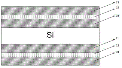
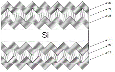
[0034](2) Prepare a composite thin film laminated passivation layer with a dielectric-metal-dielectric structure on the front and rear surfaces respectively. First, prepare a first layer of dielectric film 21 with a thickness of 1 nm to 800 nm. The materials of the dielectric layer include silicon dioxide, trioxide One or more of aluminum, silicon nitride, silicon oxynitride, and hydrogenated amorphous silicon, and then prepare a metal thin film intermediate layer with a thickness ranging from 1 nm to 400 nm by means of evaporation, sputtering, spin coating, and printing 22 , the metal...

Embodiment 2

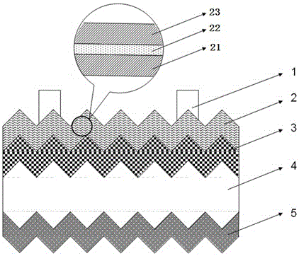
[0036] (1) Select crystalline silicon 4, crystalline silicon 4 can be p-type or n-type silicon wafers, and silicon wafers can be single crystal silicon, polycrystalline silicon or microcrystalline silicon, which are cleaned and textured in sequence to form p-n by high-temperature diffusion Junction 3, use plasma etching to remove the edge after removing the back junction;

[0037] (2) Prepare a composite thin-film laminated passivation layer 2 with a dielectric-metal-dielectric structure on the front surface. First, prepare a first layer of dielectric film 21 with a thickness of 1 nm to 800 nm. The dielectric layer material includes silicon dioxide, dioxide One or more of aluminum, silicon nitride, silicon oxynitride, and hydrogenated amorphous silicon, and then prepare a metal thin film intermediate layer with a thickness ranging from 1 nm to 400 nm by means of evaporation, sputtering, spin coating, and printing 22 , the metal here includes one or more of gold, silver, copper...

Embodiment 3

[0040] (1) Select crystalline silicon 4, which is a p-type silicon wafer with a resistivity of 1~3 Ω·cm, use 20%wt NaOH solution to polish at 80°C for 10 minutes, and then use alkaline solution to make texture to obtain a pyramid structure Finally, use RCA to clean and remove metal ions, organic matter, and particle pollutants on the surface, then use hydrofluoric acid to remove the surface oxide layer, put the silicon wafer into a tubular diffusion furnace and use phosphorus oxychloride for high-temperature diffusion at 850 ° C to form p-n Junction 3, the silicon wafer is de-junctioned after diffusion;

[0041] (2) On the front surface of the p-n junction solar cell, the ordinary SiN with a thickness of 80 nm and a refractive index of 2.1 was prepared by PECVD x : H thin film 6 is used as anti-reflection and passivation film, prepares the composite thin film lamination passivation layer 2 with dielectric-metal-dielectric structure on the rear surface of solar cell, prepares 2...


PUM

PropertyMeasurementUnit
thicknessaaaaaaaaaa
thicknessaaaaaaaaaa
thicknessaaaaaaaaaa

Abstract

The invention discloses a crystalline silicon solar cell surface passivation layer having good conductive performance. The surface passivation layer is a composite film lamination passivation layer which is disposed on the front surface and/or the back surface of a crystalline silicon solar cell and which has a dielectric-metal-dielectric structure, and the composite film lamination passivation layer comprises a first-layer medium film, a second-layer medium film and a metal film intermediate layer disposed between the first-layer medium film and the second-layer medium film. The surface passivation layer has the dielectric-metal-dielectric laminated structure and can achieve injection of current carriers into dielectrics, and the surface passivation layer has the good passivation effect and achieves a current transmission function of a surface passivation structure at the same time. The invention further discloses a method for achieving crystalline silicon solar cell surface passivation by utilizing the surface passivation layer enhancing conductivity.

Description

technical field [0001] The invention belongs to the technical field of solar cells, and in particular relates to a surface passivation layer of a crystalline silicon solar cell with good electrical conductivity and a method for passivating the surface of a crystalline silicon solar cell. Background technique [0002] At present, the thin film materials for passivation protection on the surface of crystalline silicon solar cells mainly include titanium dioxide (TiO 2 ), silicon dioxide (SiO 2 ), aluminum oxide (Al 2 o 3 ), silicon nitride (SiN x ), hydrogenated amorphous silicon (a-Si:H) and other thin film materials are prepared by thermal oxidation, evaporation, atomic layer deposition (ALD), plasma enhanced chemical vapor deposition (PECVD) and other methods after the silicon wafer is cleaned. These passivation materials are highly insulating, such as SiO 2 The resistivity is about 10 18 Ω cm, Al 2 o 3 The resistivity is about 10 15 Ω·cm. The high-resistivity t...

Claims


Application Information

Patent Timeline
Patent Type & Authority Applications(China)
IPC IPC(8): H01L31/0216H01L31/068H01L31/0224H01L31/18
CPCH01L31/02167H01L31/02168H01L31/022425H01L31/068H01L31/1868Y02E10/547Y02P70/50
Inventor 沈辉李圣浩但易
Owner 江苏润阳世纪光伏科技有限公司
Why Eureka
Try Eureka