

Composite carbon barrier coating for polysilicon ingot furnace and preparation method, graphite guard plate, polysilicon ingot furnace
A polycrystalline silicon ingot furnace and carbon coating technology, which is applied to the growth of polycrystalline materials, chemical instruments and methods, crystal growth, etc. The effect of eliminating the generation of carbon monoxide, eliminating the source of carbon pollution and improving the conversion efficiency
- Summary
- Abstract
- Description
- Claims
- Application Information
AI Technical Summary
Problems solved by technology
Method used
Image

Examples
Embodiment 1
[0030] The composite carbon barrier coating of carbon material for polysilicon ingot furnace of the present invention is used to coat the surface of carbon material devices in the ingot furnace to prevent carbon pollution, and the composite carbon barrier coating includes coating on the device surface A first coating composed of metal tungsten or metal molybdenum, and a second coating coated on the first coating, the second coating is a silicon nitride layer or consists of a silicon nitride layer and a silicon oxide layer The laminated layer, the thickness of the first coating is 0.02-300 microns, and the thickness of the second coating is 0.02-300 microns.
[0031] The composite carbon barrier coating of the present invention can be coated on one of graphite guard plate, carbon-carbon cover plate, graphite bottom plate, graphite argon gas guiding cylinder or any combination thereof.
[0032] GT-450 polycrystalline ingot casting furnace is adopted, the structure of the furnace...
Embodiment 2
[0035] A method for preparing the above composite carbon barrier coating, comprising the steps of:
[0036] S1: Ultrasonic waves are used to remove surface oil and dust on the surface of the device, and the mixed liquid of 10% hydrochloric acid and 3% hydrofluoric acid is pickled to remove surface metal and silicate impurities;
[0037] S2: Coating a layer of metal tungsten film with a thickness of 20~5000nm on the surface of the device by ion sputtering as the first coating;
[0038] S3: Coating a layer of silicon nitride film with a thickness of 20-5000 nm on the surface of the first coating by plate type PECVD as the second coating.
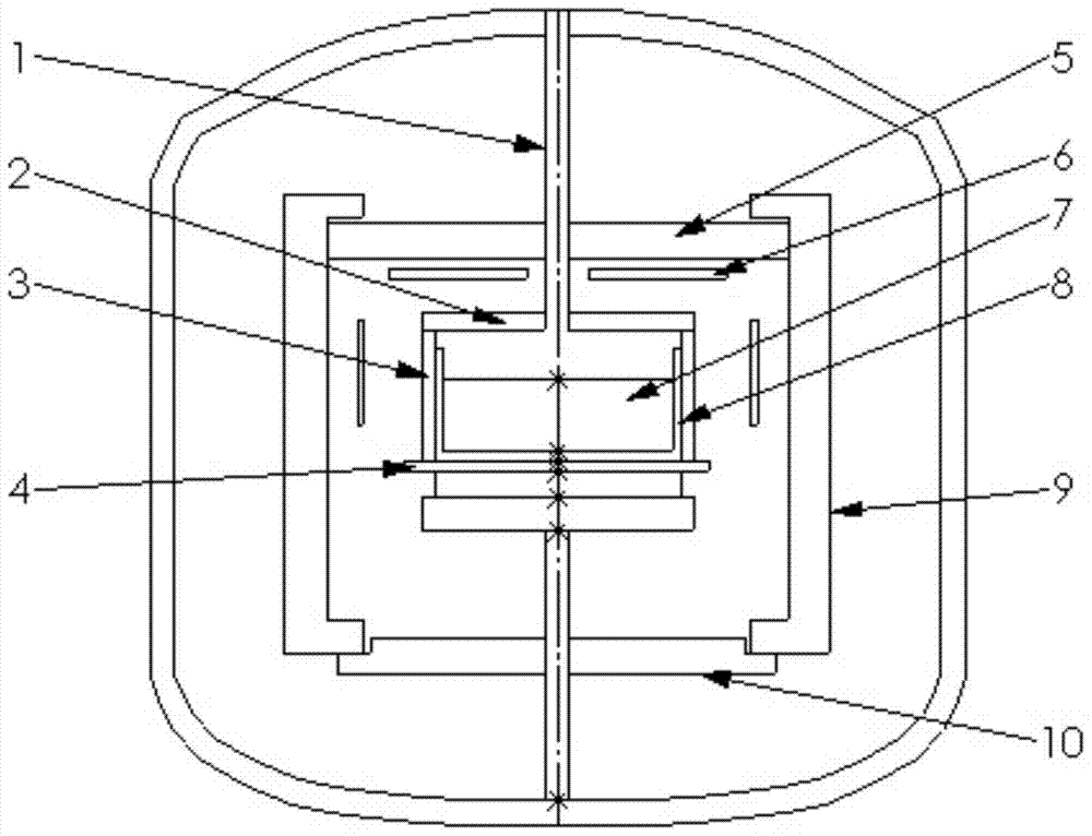
[0039] In this embodiment, the device includes a carbon-carbon cover plate 2 , a graphite shield plate 3 and a graphite bottom plate 4 . GT-450 polycrystalline ingot casting furnace is adopted, the structure of the furnace is shown in figure 1 Wrap the processed carbon-carbon cover plate 2, graphite guard plate 3, and graphite base plate 4 i...
Embodiment 3
[0041] A method for preparing the above composite carbon barrier coating, comprising the steps of:
[0042] S1: Ultrasonic waves are used to remove surface oil stains on the surfaces of carbon-carbon cover plate 2, graphite guard plate 3 and graphite bottom plate 4, and the mixed liquid of 10% hydrochloric acid and 3% hydrofluoric acid is pickled to remove surface metal and silicate impurities;
[0043] S2: Coating a metal tungsten film with a thickness of 20 to 5000 nm on the surface of the carbon-carbon cover plate 2, graphite guard plate 3 and graphite base plate 4 by ion sputtering as the first coating;
[0044] S3: Coating a layer of silicon nitride film with a thickness of 20-5000nm by plate PECVD;
[0045]S3-1: Coating a layer of silicon oxide film with a thickness of 20 to 5000 nm by plate PECVD; the stack of silicon nitride film and silicon oxide film together constitutes the second coating.
[0046] GT-450 polycrystalline ingot casting furnace is adopted, the struct...
PUM
| Property | Measurement | Unit |
|---|---|---|
| thickness | aaaaa | aaaaa |
| particle diameter | aaaaa | aaaaa |
| thickness | aaaaa | aaaaa |
Abstract
Description
Claims
Application Information