Nano-pore sensing device based on two-dimensional layer materials and configuring method thereof

A nanopore sensor, two-dimensional layered technology, applied in the direction of analytical materials, biochemical equipment and methods, specific-purpose bioreactors/fermenters, etc., can solve the problems of low sequence accuracy, high speed, and large pore thickness and other issues, to achieve the effects of solid-state nanopore stability, improved precision, easy design and array processing

Inactive Publication Date: 2016-07-20
SOUTHEAST UNIV
View PDF6 Cites 16 Cited by
  • Summary
  • Abstract
  • Description
  • Claims
  • Application Information

AI Technical Summary

Problems solved by technology

[0007] To sum up, there are still certain defects in the existing nanopore sequencing technology, such as the speed of the sequence to be

Method used


Image

  • Nano-pore sensing device based on two-dimensional layer materials and configuring method thereof
  • Nano-pore sensing device based on two-dimensional layer materials and configuring method thereof
  • Nano-pore sensing device based on two-dimensional layer materials and configuring method thereof

Examples


Embodiment 1

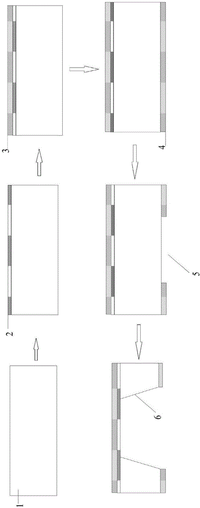
[0038] The preparation of the nanopore sensing device based on the two-dimensional layered material of the present invention specifically includes the following steps:

[0039] 1. Preparation of silicon nitride nanopores based on semiconductor Si material:

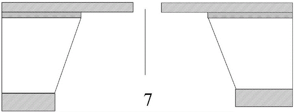
[0040] Such as Figure 2 to Figure 7 As shown, the double-sided polished 4-inch silicon wafer 1 is first cleaned with a mixed solution of concentrated sulfuric acid and hydrogen peroxide for 10-15 minutes, and then cleaned with BOE to remove silicon dioxide formed by natural oxidation on the surface of the silicon wafer. A layer of nanometer-thick silicon dioxide film 2 is formed by sputtering or thermal oxidation growth, and a layer 10 is deposited on the silicon dioxide film by Low Pressure Chemical Vapor Deposition (LPCVD) or plasma enhanced chemical deposition (PECVD). -100nm silicon nitride 3, defining this side as the front side. On the other side of the silicon wafer, a layer of silicon nitride 4 of several hundre...

Embodiment 2

[0050] Implementation steps:

[0051] 1. Select a 4-inch polysilicon wafer, and prepare a low-stress self-supporting silicon nitride film with a thickness of 30nm through silicon technology. Through focused ion beam (FIB) etching (15 seconds), or transmission electron microscope (TEM) etching (180-200 seconds), the density is 920 / μm 2 , a solid-state nanohole array with an average pore diameter of 30nm and laser-cut into a square nanohole chip with a side length of 5mm;

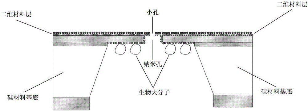
[0052] 2. A square nanohole chip with a side length of 5mm is used to grow two layers of graphene film on a clean silicon wafer by chemical vapor deposition (CVD); a transmission electron microscope (TEM) is used to etch a nanohole with a diameter of 2nm;

[0053] 3. Immerse the silicon nitride nanopore chip containing solid nanopores in a mixture containing 98% concentrated sulfuric acid and hydrogen peroxide solution (volume ratio 7:3) and heat to 95°C, hydrate for 30 minutes, so that the surface has a lar...

Embodiment 3

[0061] Implementation steps:

[0062] 1. The preparation of nanoporous base material is the same as embodiment 1;

[0063] 2. Two layers of molybdenum disulfide were grown on a clean silicon wafer with a square nanohole chip with a side length of 5 mm by chemical vapor deposition (CVD); nanoholes with a diameter of 5 nm were etched using a transmission electron microscope (TEM);

[0064] 3. Treat the nanopore array with oxygen plasma (power 100W) for 2 minutes, and ammonia plasma (power 100W) for 3 minutes to make the surface of the array carry active amino groups;

[0065] 4. Modification of glutaraldehyde as an arm molecule on the nanopore. Under the condition of weak alkaline (pH8-8.5), the aldehyde group at one end of glutaraldehyde is connected to the amino group on the wall of the nanopore to form a Schiff's base, which is then reduced by sodium borocyanide to form a stable amide bond;

[0066] 5. Use 1 μg / mL RNase antibody (anti-RNaseA) aqueous solution (containing 0....


PUM

PropertyMeasurementUnit
Average pore sizeaaaaaaaaaa
Diameteraaaaaaaaaa

Abstract

The invention discloses a nano-pore sensing device based on two-dimensional layer materials and a configuring method and application thereof.The sensing device comprises a silicon material substrate, a two-dimensional material layer, a nano-pore and biomacromolecules.The two-dimensional material layer is attached to the surface of the silicon material substrate, the nano-pore in the silicon material substrate is communicated with a small hole in the two-dimensional material layer, and the biomacromolecules are anchored to the other end of the nano-pore.Compared with the prior art, the nano-pore sensing device has the advantages that the characteristic of control over the DNA hole passing speed of the biological nano-pore and the advantages of stability, easy design and array processing of the solid nano-pore are combined, the advantage that the space resolution in nano-pore sequencing is broken through through the nano-pore manufactured through the two-dimensional layer materials is adopted, and the nanometer device capable of directly conducting efficient information reading on an analyte is developed so that the requirement for reading DNA encoding information in current medical and future information devices can be met, and the accuracy of nano-pore sequencing is improved.

Description

technical field [0001] The invention relates to a nanopore sensor device based on a two-dimensional layered material and a construction method thereof, belonging to the technical field of nanometer sensor devices. Background technique [0002] Nanopores are used in the detection of biomolecules through electrophoresis to drive a biomolecule through a small hole with a diameter of several nanometers. In 1996, Kasianowicz and his colleagues reported for the first time that single-stranded DNA or RNA passed through the α-hemolysin nanopore self-assembled on the lipid bilayer under the action of an electric field, and changed the conductance of the nanopore when the DNA molecule passed through the pore, The current changes, resulting in the phenomenon of blocking current (blockadecurrent). Since different bases have different atomic compositions, they will generate different blocking currents when passing through the nanopore. According to the detectable signal, four different ...

Claims


Application Information

Patent Timeline
IPC IPC(8): C12M1/34
CPCG01N33/48721
Inventor 陆祖宏刘全俊陈云飞巴龙谢骁汪荣亮
Owner SOUTHEAST UNIV
Why Eureka
Try Eureka