

Ultra-thin silver base thin film, multi-layer composite transparent electric conduction thin film and preparing method and application thereof
A transparent conductive film, multi-layer composite technology, applied in the coating, superimposed layer plating, metal material coating process and other directions, can solve the photoelectric performance island growth mode and aging effect, the oxygen doping concentration is difficult to accurately control, the preparation conditions of the conductive film are harsh and other problems, to achieve the effect of convenient application, good mechanical flexibility, and good mechanical flexibility
- Summary
- Abstract
- Description
- Claims
- Application Information
AI Technical Summary
Problems solved by technology
Method used
Image

Examples
Embodiment 1
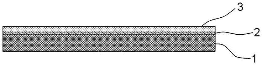
[0063] Such as figure 1 As shown, an ultra-thin silver-based film includes Ag(O) layer 2 and Ag layer 3, Ag(O) layer 2 is located on substrate 1, Ag layer 3 is located on Ag(O) layer 2 and is connected with Ag(O) layer 2 touch. The total thickness of the Ag(O) / Ag bilayer film is preferably 3 nm to 12 nm, wherein the thickness of the Ag(O) layer 2 is 0.5 to 5 nm, preferably 1 nm to 3 nm. The thickness of the Ag layer 3 is 2 nm to 10 nm, preferably 3 nm to 7 nm. In the Ag(O) layer 2 , the oxygen doping concentration x satisfies 1≦x≦24%, preferably, 2%≦x≦15%.
[0064] Substrate 1 can be a dielectric, semiconductor or metal substrate, including glass, quartz, silicon wafer, stainless steel, etc.; it can also be an organic polymer substrate, including polyethylene terephthalate (PET), polyethylene naphthalate Various resin films such as ethylene glycol ester (PEN), polycarbonate (PC), polyimide (PI), ethylene-tetrafluoroethylene copolymer (ETFE), and heat-resistant transparent f...
Embodiment 2
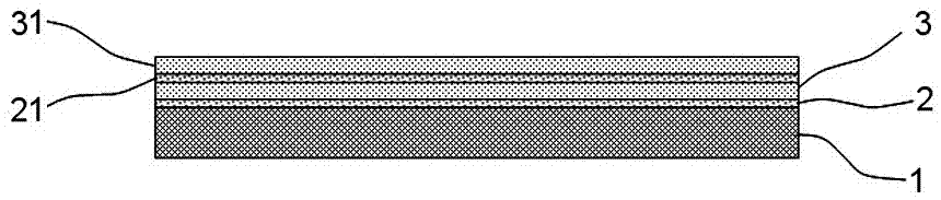
[0070] Such as figure 2 As shown, a multilayer composite transparent conductive film includes a substrate 1 and at least two layers of Ag(O) / Ag double-layer stacking structure, specifically, a first Ag(O) layer 2, a second layer of Ag(O) are sequentially arranged on the substrate 1 An Ag layer 3 , a second Ag(O) layer 21 and a second Ag layer 31 .
[0071] The preparation method of multilayer composite transparent conductive film is as follows:
[0072] (1) Put the substrate 1 on the substrate stage in the cavity of the magnetron sputtering thin film deposition equipment pre-installed with the high-purity Ag target;
[0073] (2) Pump the background vacuum of the cavity of the magnetron sputtering equipment to 1.0×10 -3 Below Pa, argon and an appropriate amount of oxygen are introduced into the cavity, and a high-purity Ag target is sputtered under an argon-oxygen mixed gas atmosphere, and a first Ag(O) layer 2 is deposited on the substrate 1;
[0074] (3) Without breaking ...
Embodiment 3
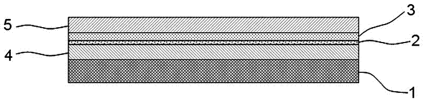
[0078] Such as image 3 Shown, a kind of multilayer composite transparent conductive film comprises substrate 1, Ag (O) layer 2, Ag layer 3, bottom layer 4 and top layer 5, wherein, bottom layer 4 is arranged between substrate 1 and Ag (O) layer 2, It is used for enhanced adhesion, work function matching, protection, anti-reflection or any combination of these properties; the top layer 5 is disposed on top of the Ag layer 3 which is used for anti-reflection, work function matching, protection or any combination of these properties.
[0079] Substrate 1 can be a dielectric, semiconductor or metal substrate, including glass, quartz, silicon wafer, stainless steel, etc.; it can also be an organic polymer substrate, including polyethylene terephthalate (PET), polyethylene naphthalate Various resin films such as ethylene glycol ester (PEN), polycarbonate (PC), polyimide (PI), ethylene-tetrafluoroethylene copolymer (ETFE), and heat-resistant transparent films and laminates with orga...
PUM
| Property | Measurement | Unit |
|---|---|---|
| Thickness | aaaaa | aaaaa |
| Thickness | aaaaa | aaaaa |
| Total thickness | aaaaa | aaaaa |
Abstract
Description
Claims
Application Information