Novel oxidizing-resistant nanometer copper soldering paste and preparation method and application thereof

An anti-oxidation and nano-copper technology, applied in transportation and packaging, metal processing equipment, ion implantation plating, etc., can solve problems such as reducing joint strength and interface strength, accelerating copper oxidation, and affecting sintering quality, so as to improve sintering quality , the effect of improving the strength of the joint and improving the conductivity

Inactive Publication Date: 2017-10-20
UNIV OF SHANGHAI FOR SCI & TECH
View PDF7 Cites 10 Cited by
  • Summary
  • Abstract
  • Description
  • Claims
  • Application Information

AI Technical Summary

Problems solved by technology

[0006] However, the problem of easy oxidation of nano copper solder paste has been difficult to solve
The high activity of nano-metal particles accelerates the oxidation of copper. Even if it is stored at low temperature, it is difficult to stop the oxidation process. The oxide film on the surface of nano-copper particles not only directly affects the electrical conductivity, but also reduces the electrical performance of the joint after sintering; at the same time, the oxide film also affects the sintering quality between particles. And then reduce the joint strength and interface strength
The more effective anti-oxidation methods in the existing research mainly adopt methods such as adjusting the organic passivation layer, controlling the sintering atmosphere, rapid sintering, and increasing the silver coating layer, including a nano-silver coated copper powder proposed by Harbin Institute of Technology Low-temperature sintering solder paste (publication number: CN103521945A), however, the effect is not significant in terms of cost, controllability, and ease of operation

Method used


Image

  • Novel oxidizing-resistant nanometer copper soldering paste and preparation method and application thereof
  • Novel oxidizing-resistant nanometer copper soldering paste and preparation method and application thereof
  • Novel oxidizing-resistant nanometer copper soldering paste and preparation method and application thereof

Examples


Embodiment 1

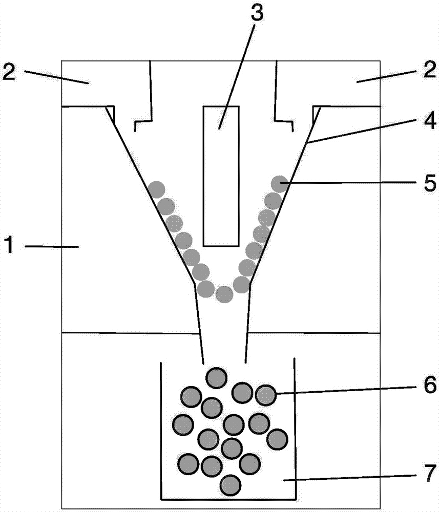
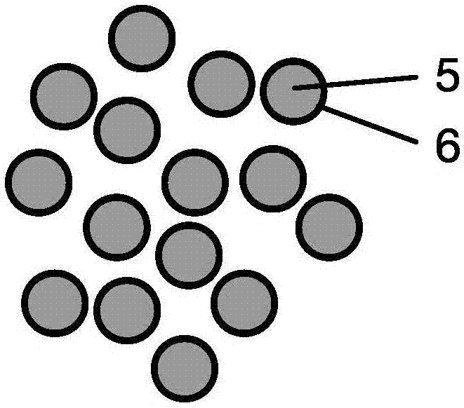
[0041] Step 1, such as figure 1 The magnetron sputtering method is used to prepare the coated nano-copper powder particles. Take the spherical nano-copper powder with a particle diameter of 20-80nm and pour it into the inverted cone-shaped rotatable lower hopper 4 through the feeding chamber 2. The nano-copper powder 5 moves in a spiral in the rotatable lower hopper 4 and falls into the magnetron sputtering. The process vacuum generation chamber 1 bombards the columnar silver or gold columnar target 3 with gas ions, knocks out its atoms and deposits them on the surface of the nano-copper powder 5 to form a silver or gold metal coating 6 . Among them, the rotation rate of the rotatable lower hopper 4 is controlled by the motor, and then the rotation rate of the nano-copper powder is controlled; the coating thickness is controlled by controlling the magnetron sputtering process parameters, including the sputtering angle and incident energy; thus, uniform A consistent metal coat...

Embodiment 2

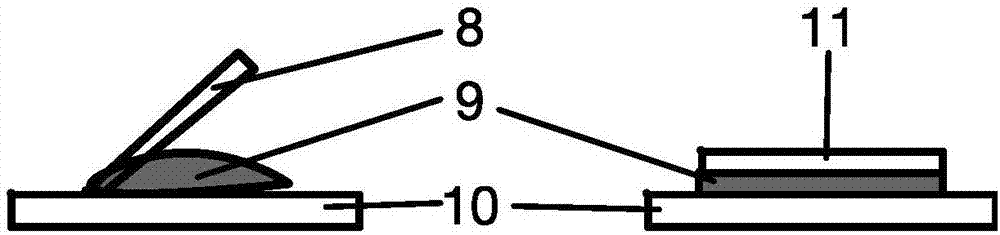
[0046] like image 3 and Figure 4 As shown, the new anti-oxidation nano-copper solder paste 9 prepared in Example 1 is coated on the substrate 10 by a screen printing process with a scraper 8 , and the chip or device 11 is surface mounted. Place the mounted sample on the heating plate 13, fill the sintering furnace cavity 19 with argon through the air inlet 15, set the temperature of the heating plate 13 to 150°C, and preheat for 2 minutes. Then, the gas inside the sintering furnace cavity 19 is discharged from the gas outlet 16 through the vacuum pump 17, and the pressure in the sintering furnace cavity 19 is adjusted through the vacuum gauge 18 to form a negative pressure; at this time, the temperature of the heating plate 13 is quickly raised to 310° C. Hold for 15 minutes to complete the sintering process and form a strong interconnection joint.

Embodiment 3

[0048] like image 3 and Figure 4 As shown, a new anti-oxidation nano-copper solder paste 9 is coated on a substrate 10 by a screen printing process with a scraper 8 , and a chip or device 11 is surface mounted. Place the mounted sample on the heating plate 13, fill the sintering furnace cavity 19 with argon gas through the air inlet 15, set the temperature of the heating plate to 150°C, and move the movable support 12 upward until the sample touches the fixed Push the pillar 14 and apply a pressure of 5 MPa, rapidly raise the temperature to 220° C. and keep it for 10 minutes to complete the sintering process and form a firm interconnection joint.

[0049] The chip was mounted on the substrate using traditional nano-copper solder paste, and it was raised from room temperature to 200 °C under nitrogen atmosphere and kept for 10 minutes. The joint shear strength obtained under different heating rates was as follows: Figure 5 As shown, the highest is 5MPa; or directly sintere...


PUM

PropertyMeasurementUnit
diameteraaaaaaaaaa
thicknessaaaaaaaaaa

Abstract

The invention relates to novel oxidizing-resistant nanometer copper soldering paste and a preparation method and application thereof. By adopting a magnetron sputtering process, the surface of nanometer copper powder is evenly coated with a metal film. Silver, gold and the like can be selected as the components of the metal film as required; then a traditional nanometer copper soldering paste formula continues to be used, a proper amount of forming auxiliaries are added; and finally, the novel oxidizing-resistant nanometer copper soldering paste resistant to oxidizing and cracks is prepared. Compared with the prior art, according to the novel nanometer copper soldering paste, mutual connection between a chip and a substrate can be achieved by means of a low-temperature sintering process or a pressurizing low-temperature sintering process, a traditional nanometer copper soldering paste function is achieved; and oxidizing resistance, crack initiation resistance and an extending performance are achieved at the same time, the novel oxidizing-resistant nanometer copper soldering paste can be used in large-power high-temperature electronic device packaging, and is especially suitable for packaging of third-generation semiconductor devices, after packaging, a connector is good in performance, fault-free service under high temperature can be achieved for a long time, and the novel nanometer copper soldering paste is matched with an existing lead-free solder packaging process.

Description

technical field [0001] The invention relates to the field of electronic packaging and interconnection materials, in particular to a novel anti-oxidation nano-copper solder paste and its preparation method and application. Background technique [0002] Power semiconductor devices are mainly developing towards three-dimensional heterogeneous integration and high switching frequency. The essential problems are reflected in high power density, high temperature applications, high reliability requirements and system miniaturization; especially in automotive electronics, turbines, aerospace, industrial electronics, deep wells Devices in fields such as mining are faced with high-temperature application requirements, and the extreme ambient temperature is mostly above 300°C. The maximum junction temperature of traditional silicon devices is 150-200°C, which is difficult to meet its needs. However, the operating junction temperature of SiC and other wide bandgap semiconductor devices ...

Claims


Application Information

Patent Timeline
Patent Type & Authority Applications(China)
IPC IPC(8): C23C14/35C23C14/16B22F1/02H01L23/488
CPCH01L24/13C23C14/165C23C14/35H01L2224/13147H01L2224/13444H01L2224/13439B22F1/17
Inventor 徐玲
Owner UNIV OF SHANGHAI FOR SCI & TECH
Why Eureka
Try Eureka