Lead selenide nanorod, preparation method and application thereof in field effect transistor

A technology of nanorods and lead selenide, applied in nanotechnology, nanotechnology, binary selenium/tellurium compounds, etc., can solve the problem of difficulty in lead selenide nanorods, insufficient uniformity of size, and dissolution of lead selenide nanorods Insufficient solubility and other problems, to achieve good solubility, uniform size distribution, high performance

Active Publication Date: 2018-03-13
SUZHOU UNIV
View PDF6 Cites 2 Cited by
  • Summary
  • Abstract
  • Description
  • Claims
  • Application Information

AI Technical Summary

Problems solved by technology

[0003] However, field effect transistors based on lead selenide nanometers are rarely studied at present, and such materials have electron and hole mobilities in the range of 10 -4 cm 2 / Vs around
In particular, the research on the mechanism of charge transport performance under variable temperature conditions has not been reported, and the solution of this problem will help the material to be more widely used in optoelectronic devices
Also because the crystal structure of lead selenide is a highly symmetrical cube, it is more difficult to anisotropically grow lead selenide nanorods with one-dimensional structure. Therefore, the solubility of the obtained lead selenide nanorods is not ideal enough, and the uniformity of size There are also deficiencies
At present, high-performance field-effect transistors based on lead selenide nanorods have not been reported

Method used


Image

  • Lead selenide nanorod, preparation method and application thereof in field effect transistor
  • Lead selenide nanorod, preparation method and application thereof in field effect transistor
  • Lead selenide nanorod, preparation method and application thereof in field effect transistor

Examples


Embodiment 1

[0037] In this example, the lead selenide nanorods were synthesized at a temperature of 100°C. The specific steps are as follows:

[0038] (1) Preparation of lead precursor: under the protection of nitrogen, add 89 mg (0.4 mmol) of lead oxide, 170 mg (1 mmol) of trans-2-decenoic acid and 8 g of octadecene into a 50 mL three-necked flask In the three-necked flask, stir for 1 hour at 120 ℃ until the solution becomes clear and transparent, and then vacuumize at 100 ℃ for 1 hour to remove the water and oxygen in the three-necked flask to obtain the lead precursor, which is ready for use;

[0039] (2) Reaction at preset temperature: Dissolve 20 μL of diphenylphosphine and 1.2 mL of selenium tris (diethylamino) phosphine solution (molar concentration of 1 mol / L) in 1.2 mL of octadecene and mix well Then use a syringe to quickly inject it into the above-mentioned lead precursor pre-adjusted to 100 ℃, and react for 10 minutes;

[0040] (3) Post-treatment: After cooling to room temperature w...

Embodiment 2

[0045] This embodiment provides a field effect transistor device based on lead selenide nanorods.

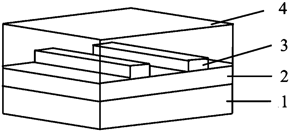
[0046] See attached image 3 , It is a schematic diagram of the structure of the lead selenide nanorod field effect transistor device provided in this embodiment. The field-effect transistor is a layered structure, from bottom to top including n-type doped silicon wafer 1, and silicon dioxide (SiO) attached to the n-type doped silicon wafer. 2 ) Layer 2, with SiO 2 The gold (Au) electrode layer 3 is bonded to each other, and the lead selenide nanorod layer 4 is bonded to the substrate.

[0047] The ultra-fine lead selenide nanorod field effect tube device provided in this embodiment is prepared by the following preparation method: in a highly purified environment, vapor deposition technology is used to deposit a certain thickness on the surface of the n-type doped silicon wafer 1 Silicon dioxide (SiO 2 ) Layer 2; using planar magnetron technology, sputtering gold (Au) electrode layer...

Embodiment 3

[0056] This embodiment provides a field effect transistor device based on lead selenide nanorods, and its structure is shown in Appendix image 3 . The deposited gold electrode layer and deposited SiO 2 After cleaning the n-type doped silicon wafers, spin-coated the PbSe nanorod n-hexane solution prepared in Example 1, and after ligand exchange, evaporate 80nm thick Cu to obtain.

[0057] In this embodiment, the concentration of the n-hexane solution of the lead selenide nanorods is 15-25mg / mL, preferably 20mg / mL, the rotation speed during spin coating is 1000-2000rpm, preferably 1000rpm, and the duration is 15-30s, preferably 30s, Spin coating 3 layers.

[0058] In this embodiment, the ligand exchange reagent is tetra-n-butyl ammonium iodide (the ligand is also tetra-n-butyl ammonium bromide or tetra-n-butyl ammonium chloride) dissolved in anhydrous methanol with a concentration of 25 to 35 mM, preferably 30 mM, ligand exchange 20-40 s, preferably 30 s.

[0059] The performance in...


PUM

PropertyMeasurementUnit
diameteraaaaaaaaaa
lengthaaaaaaaaaa

Abstract

The invention discloses a lead selenide nanorod, a preparation method and application thereof in a field effect transistor. The preparation method includes: using lead selenide and trans-2-caproleic acid as raw materials to prepare a lead precursor; performing reaction and aftertreatment to obtain the lead selenide nanorod. A molecular formula is PbSe, a surface ligand is organic acid-trans-2-caproleic acid, and band gap is 1.03 electron volt. The lead selenide nanorod is applied to the field effect transistor, an inorganic ligand-tetrabutylammonium halide is enabled to exchange an organic acid ligand on the surface of the lead selenide nanorod, electrical performance of the lead selenide nanorod shows bipolarity, electron mobility measured in vacuum is 0.1cm2 / Vs, and hole mobility is 1.1x10⁻⁴cm2 / Vs. in 50-297K heterotherm, charge transfer mechanism at 200K is changed from nearest transition mechanism into transition mechanism in a variable area, charge transmission is dominated by a highly-disorderly state, and the lead selenide nanorod can be widely applied in the field of solar cells and photoelectric detectors.

Description

Technical field [0001] The invention relates to a lead selenide semiconductor nanorod, a preparation method and its application in a field effect transistor, belonging to the technical field of optoelectronic materials. Background technique [0002] Lead selenide (PbSe) in lead chalcogenide semiconductors has a large Bohr radius, which makes its quantum confinement effect particularly significant, and has properties such as large absorption coefficient, high electron mobility, and adjustable energy level. The excellent properties of lead selenide nanocrystals make it a more popular photovoltaic nanomaterial in current research, and the one-dimensional structure of lead selenide has more effective charge transport and multiple excitons in optoelectronic devices than the zero-dimensional structure. The efficiency is doubled and the anisotropic optical absorption is advantageous. In 2014, the document "Preparation of ultrafine lead selenide nanorods and its application in photovolt...

Claims


Application Information

Patent Timeline
Patent Type & Authority Applications(China)
IPC IPC(8): C01B19/04H01L29/24H01L29/775H01L21/34B82Y30/00
CPCB82Y30/00C01B19/007C01P2002/72C01P2002/84C01P2004/04C01P2004/64H01L29/245H01L29/66439H01L29/775
Inventor 马万里韩璐
Owner SUZHOU UNIV
Why Eureka
Try Eureka