Method for crystallizing germanium antimony tellurium materials through electronic beam irradiation induction

A technology of electron beam irradiation, germanium antimony tellurium, applied in metal material coating process, ion implantation plating, coating and other directions, can solve the problem of phase change material stay, etc., to facilitate in-situ observation and microstructure characterization, Achieve the effect of in-situ performance testing

Active Publication Date: 2018-09-28
XI AN JIAOTONG UNIV
View PDF3 Cites 3 Cited by
  • Summary
  • Abstract
  • Description
  • Claims
  • Application Information

AI Technical Summary

Problems solved by technology

However, limited by the limitations of experimental equipment at this stage, most of the research on phase change materials in the reports has always remained at the ex-situ stage. People have used X-ray diffraction (XRD), X-ray absorption fine structure spectroscopy (EXAFS), Indirect measurements s

Method used


Image

  • Method for crystallizing germanium antimony tellurium materials through electronic beam irradiation induction
  • Method for crystallizing germanium antimony tellurium materials through electronic beam irradiation induction
  • Method for crystallizing germanium antimony tellurium materials through electronic beam irradiation induction

Examples


Embodiment 1

[0045] In this implementation, the phase change material GeSb 2 Te 4 As an example, a cubic phase nanograin with a grain size of about 30nm is prepared, and the sample is prepared on a TEM standard copper grid for easy observation. The specific process is as follows:

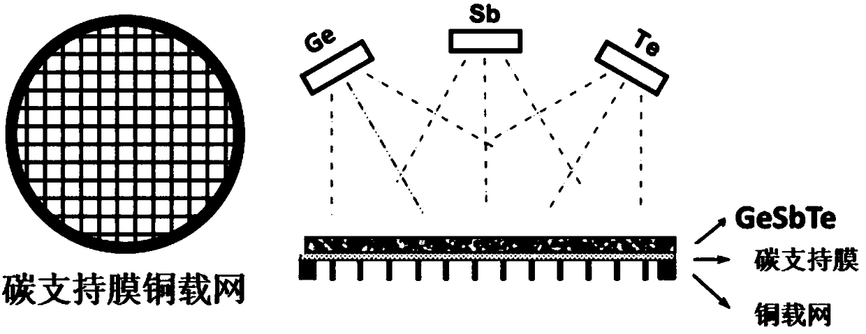
[0046] Step 1: Select a TEM standard size copper grid with an ultra-thin carbon support film (3-5nm) on the surface as the film substrate, and deposit 80nm thick GeSb by magnetron sputtering 2 Te 4 Amorphous thin films (such as figure 1 shown).

[0047] Step 2: Load the sample onto the TEM sample holder and perform plasma cleaning.

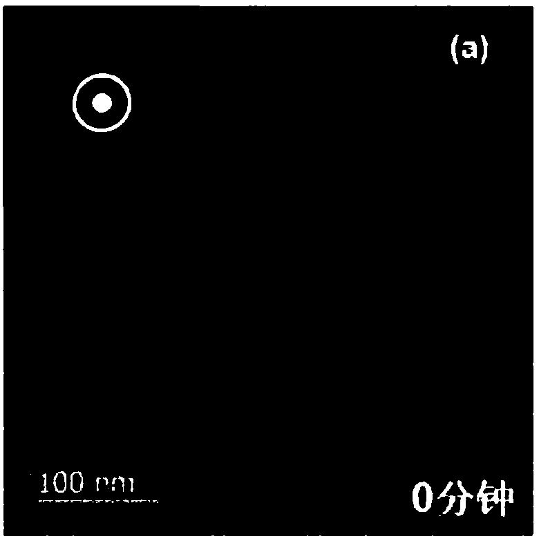
[0048] Step 3: Use TEM to find a clean and flat area on the film, as shown in Figure 3(a).

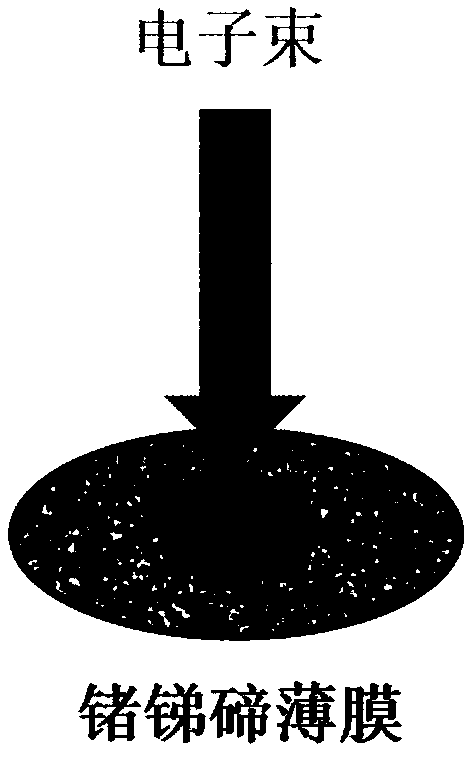
[0049] Step 4: Set the TEM voltage to 200kV, focus the electron beam to 0.3μm, and set the electron beam intensity to 1×10 25 m -2 the s -1 ,Such as figure 2 shown.

[0050] Step 5: Observe the crystallization process in real time (as shown in Figure 3(a)-(d)), after 10 minutes th...

Embodiment 2

[0053] In this implementation, the phase change material Ge 2 Sb 2 Te 5 As an example, cubic phase nanocrystals with a grain size of about 35nm were prepared, and the samples were prepared on silicon wafers for electrical performance testing. The specific process is as follows:

[0054] Step 1: Select a silicon wafer as a thin film substrate, and deposit 200nm thick Ge by molecular beam epitaxy 2 Sb 2 Te 5 Amorphous thin film.

[0055] Step 2: Using ion thinning technology to perform electron microscope sample pretreatment on the substrate for preparing the germanium antimony tellurium amorphous thin film, the thickness of the sample is 90nm.

[0056] Step 3: Use an electron microscope to find a clean and flat area on the film.

[0057] Step 4: Set the electron microscope voltage to 200kV, focus the electron beam to 1μm, and set the electron beam intensity to 1×10 23 m -2 the s -1 .

[0058] Step 5: Observe the crystallization process in real time. After 40 minutes, ...

Embodiment 3

[0061] In this implementation, the phase change material GeSb 2 Te 4 As an example, a hexagonal phase nanograin with a grain size of about 300nm was prepared, and the sample was prepared on a heating chip for external field loading experiments. The specific process is as follows:

[0062] Step 1: Select the heated chip as the thin film substrate, and deposit GeSb with a thickness of 70nm by physical vapor deposition 2 Te 4 Amorphous thin film.

[0063] Step 2: Using focused ion beam technology to perform electron microscope sample pretreatment on the substrate for preparing the germanium antimony tellurium amorphous thin film.

[0064] Step 3: Use an electron microscope to find a clean and flat area on the film.

[0065] Step 4: Set the electron microscope voltage to 120kV, focus the electron beam to 5μm, and set the electron beam intensity to 1×10 26 m -2 the s -1 .

[0066] Step 5: Observe the crystallization process in real time under in-situ heating conditions. Aft...


PUM

PropertyMeasurementUnit
Thicknessaaaaaaaaaa

Abstract

The invention discloses a method for crystallizing germanium antimony tellurium materials through electronic beam irradiation induction. The method comprises the steps that a substrate capable of carrying out microstructure representation or electrical property testing or in-situ performance testing is selected for preparing a germanium antimony tellurium amorphous film; the substrate for preparing the germanium antimony tellurium amorphous film is subjected to electron microscope sample pretreatment; a clean and smooth area of the surface of the germanium antimony tellurium amorphous film isfound in an electron microscope sample; the irradiation range, irradiation voltage, irradiation intensity and irradiation time are set in an electron microscope; the crystallizing process of the irradiation area of the electron microscope sample is observed in the electron microscope in real time, germanium antimony tellurium crystals meeting the crystallizing range, the crystal structure and thegrain size are obtained, and the process of crystallizing the germanium antimony tellurium materials through electronic beam irradiation induction is completed. The method provides experimental evidences for the study of the phase-change material crystallization mechanism and corresponding structural performance.

Description

technical field [0001] The invention relates to a method for crystallizing novel germanium, antimony and tellurium materials, in particular to a method for inducing crystallization of germanium, antimony and tellurium materials by electron beam irradiation. Background technique [0002] As the next generation of non-volatile memory, phase change memory has broad development space and application prospects in the field of information storage. Phase change memory has shown great advantages in size scalability, power consumption, and compatibility. Phase change memory (PRAM) based on phase change materials (PCMs) and resistive change memory (RRAM) based on resistive oxides Magneto-resistive memory (MRAM) of spintronic materials is considered to be the most likely to replace the current SRAM, DRAM and FLASH, and become the mainstream non-volatile memory in the future. They not only have high storage density, but also have the read and write speed of memory DRAM and the non-vola...

Claims


Application Information

Patent Timeline
IPC IPC(8): C23C14/58C23C14/06
CPCC23C14/0623C23C14/582
Inventor 张伟王疆靖田琳
Owner XI AN JIAOTONG UNIV
Why Eureka
Try Eureka