Zinc oxide ultraviolet photoelectric detector with adjustable gate voltage and preparation method thereof
An electrical detector, zinc oxide technology, applied in the field of zinc oxide ultraviolet photodetector and its preparation, can solve the problem of inability to apply an external electric field for carrier concentration regulation, inability to achieve arbitrary heterogeneity integration, and inability to meet two-dimensional silicon-based optoelectronics Problems such as the need for large-area integration of devices
- Summary
- Abstract
- Description
- Claims
- Application Information
AI Technical Summary
Problems solved by technology
Method used
Image
Examples
Embodiment 1
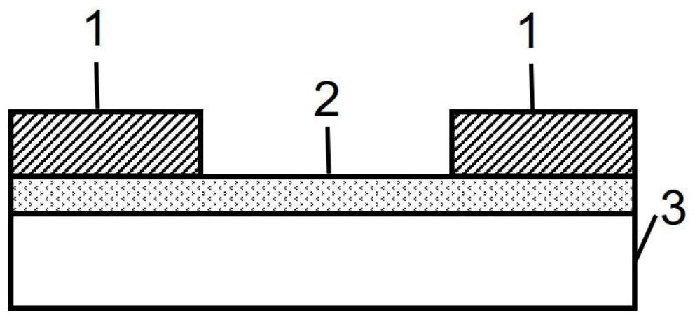
[0066] An ultra-thin zinc oxide ultraviolet photodetector with adjustable gate voltage, which is composed of a metal electrode 1, a two-dimensional zinc oxide nanosheet layer 2 and an insulating silicon substrate 3; specifically as figure 1 As shown, wherein, the two-dimensional zinc oxide nanosheet layer 2 covers the surface of the insulating silicon substrate 3; the metal electrode 1 is arranged on the surface of the two-dimensional zinc oxide nanosheet 2, the metal electrode is a pure gold metal electrode, and the thickness of the metal electrode is 60 nm; the distance between the two metal electrodes 1 is 5 μm, and the width of the two metal electrodes 1 is 5 μm.
[0067] The preparation method is:
[0068] (1) Preparation of two-dimensional zinc oxide nanosheets by ion layer epitaxy: Cut the insulating silicon wafer into 1cm×1cm, measure 3mL of hydrogen peroxide solution with a volume fraction of 30%, and slowly pour it into 7mL of concentrated sulfuric acid to prepare P...
Embodiment 2
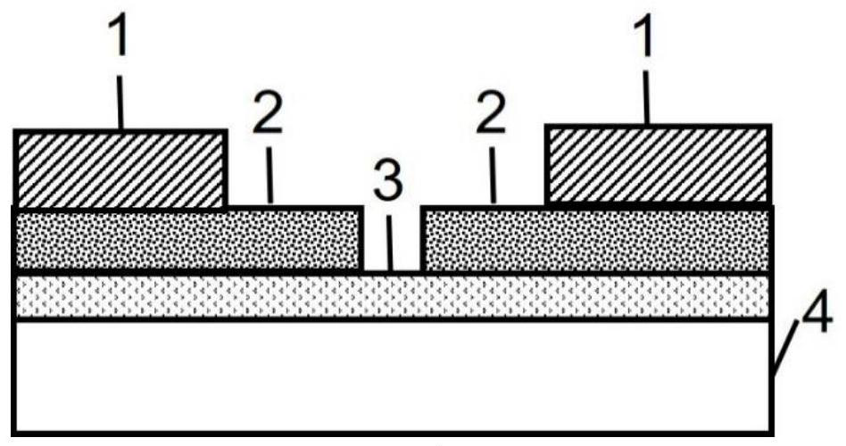
[0072] An ultra-thin zinc oxide ultraviolet photodetector with adjustable gate voltage, which is composed of a metal electrode 1, a two-dimensional material 2, a two-dimensional zinc oxide nanosheet 3 and an insulating silicon substrate 4; specifically as image 3As shown, wherein, the two-dimensional zinc oxide nanosheet 3 is covered on the surface of the insulating silicon substrate 4; the two-dimensional material 2 with metallic or semi-metallic properties is covered on the surface of the zinc oxide nanosheet 3; the metal electrode 1 is set On the surface of the two-dimensional material 2 with metallic or semi-metallic properties, the metal electrode is a chromium / gold electrode with a thickness of 10nm (two-dimensional material) / 50nm (metal electrode); the distance between the two metal electrodes 1 is 10 μm, and the two The pitch of the two-dimensional material 2 is 5 μm. The distance between the metal electrodes 1 can be equal to or greater than the distance between the ...
Embodiment 3
[0082] A zinc oxide ultraviolet photodetector with adjustable grid voltage and its preparation method are the same as in Example 2, except that the two-dimensional electrode material is tungsten disulfide in 1T' phase.
[0083] The preparation method is:
[0084] (1) Preparation of zinc oxide nanosheets by ion layer epitaxy: Cut the insulating silicon wafer into 1cm×1cm, measure 3mL of hydrogen peroxide solution with a volume fraction of 30%, and slowly pour it into 7mL of concentrated sulfuric acid to prepare piranhas solution. Place the insulating silicon chip in the piranha solution, place it on a hot plate at 80°C and heat it for 20 minutes for hydrophilic treatment, and then clean the silicon chip with plenty of water. Prepare anionic surfactant with sodium lauryl sulfate solution and deionized water at a volume ratio of 1:500, weigh zinc nitrate and hexamethylenetetramine at a molar ratio of 1:1, and dissolve them in deionized water to obtain a reaction solution a, mak...
PUM
| Property | Measurement | Unit |
|---|---|---|
| Thickness | aaaaa | aaaaa |
| Thickness | aaaaa | aaaaa |
| Total thickness | aaaaa | aaaaa |
Abstract
Description
Claims
Application Information


