Preparation method of bamboo holocellulose nanofiber with high length-diameter ratio and high hemicellulose content
A technology of hemicellulose and nanofibers, applied in the direction of cellulose/protein conjugated artificial filaments, nanotechnology, fiber chemical characteristics, etc. low, can not fully meet the needs of use, etc., to achieve the effect of environmental friendliness, short time and easy operation
- Summary
- Abstract
- Description
- Claims
- Application Information
AI Technical Summary
Problems solved by technology
Method used
Image

Examples
Embodiment 1
[0033] The preparation method of the bamboo heddled cellulose nanofiber with high aspect ratio and high hemicellulose content, the steps are as follows:
[0034] (1) Preparation of deep eutectic solvent (DES): zinc acetate (ZA) was used as hydrogen bond donor, choline chloride (ChCl) was used as hydrogen bond acceptor, and the molar ratio of donor and acceptor was 1:2. , the mixture was heated at 80 °C with magnetic stirring for 4 h until a homogeneous clear liquid appeared.
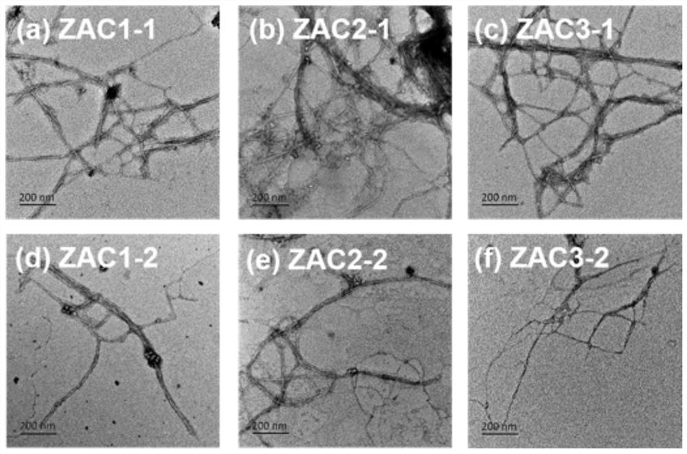
[0035] (2) Pretreatment: Add 0.5 g bamboo cellulose powder and 25 mL zinc acetate / choline chloride (ZAC) to the Teflon container of the microwave reactor. The solid-liquid ratio of bamboo cellulose powder and DES is 1:50 (g / mL), and acetic acid is added, and the molar ratio of acetic acid and DES is 1:1 (ZAC1-1) or 1:2 (ZAC2-1) , or 1:3 (ZAC3-1). Use a glass rod to stir to mix well. The mixture was treated at 120° C. for 10 minutes under a microwave irradiation power of 600 W. After pretreatment, the...
Embodiment 2
[0038] The preparation method of the bamboo heddled cellulose nanofiber with high aspect ratio and high hemicellulose content, the steps are as follows:
[0039] (1) Preparation of deep eutectic solvent (DES): zinc acetate (ZA) was used as hydrogen bond donor, choline chloride (ChCl) was used as hydrogen bond acceptor, and the molar ratio of donor and acceptor was 1:2. , the mixture was heated at 80 °C with magnetic stirring for 4 h until a homogeneous clear liquid appeared.
[0040] (2) Pretreatment: Add 0.5 g bamboo cellulose powder and 25 mL zinc acetate / choline chloride (ZAC) to the Teflon container of the microwave reactor. The solid-liquid ratio of bamboo cellulose powder and DES is 1:50 (g / mL), and acetic acid is added, and the molar ratio of acetic acid and DES is 1:1 (ZAC1-2), or 1:2 (ZAC2-2) , or 1:3 (ZAC3-2). Use a glass rod to stir to mix well. The mixture was treated at 140° C. for 10 minutes under a microwave irradiation power of 600 W. After pretreatment, th...
Embodiment 3
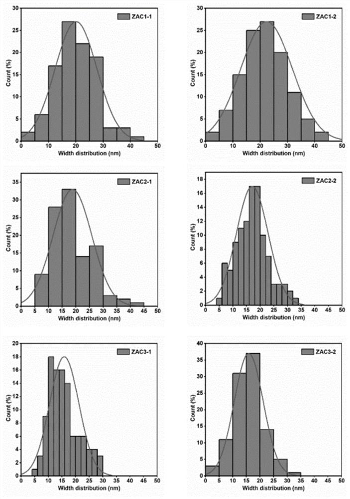
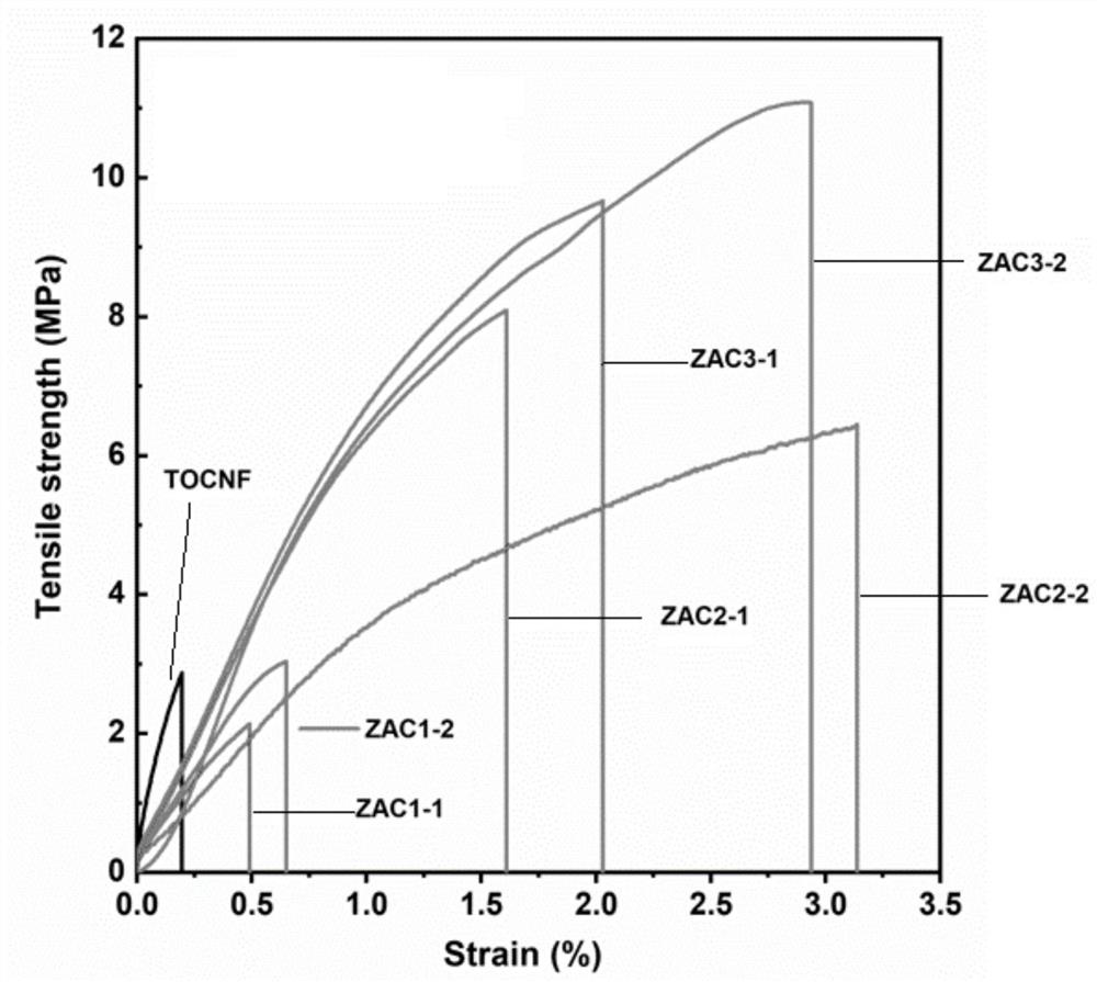
[0043] Six HCNF products named ZAC1-1, ZAC2-1, (ZAC3-1, ZAC1-2, ZAC2-2, ZAC3-2) prepared in Examples 1 and 2 were characterized, and the results are shown in Table 1. The specific method is as follows:
[0044] 1) The formula for calculating the recovery rate is: recovery rate=HCNF mass (g) / bamboo cellulose powder mass (g)*100%.
[0045] 2) AFM observation: Dilute the suspension of nanofiber cellulose by 0.5%, and drop it on a smooth mica sheet. After natural air-drying, use an atomic force microscope to observe the morphology of nanofibers, and obtain the average length (nm), average width (nm) and length Diameter ratio.
[0046] 3) Determination of crystallinity: the instrument used is X-ray diffractometer, crystallinity (%)=peak area of crystalline region / (peak area of crystalline region+peak area of amorphous region)*100%.
[0047] 4) Determination of dextran and xylan content: adopt the special lignocellulosic component determination method of American Energy Labo...
PUM
 Abstract
Description
Claims
Application Information