Method for patterning thin films

a thin film and patterning technology, applied in the direction of loop antennas, printing, thermography, etc., can solve the problems of sudden increase in surface temperature for a short time, inability to achieve the desired effect, and inability to produce debris. , to achieve the effect of reducing process steps, reducing the generation of debris, and high fluen

Inactive Publication Date: 2001-07-05
3M INNOVATIVE PROPERTIES CO
View PDF0 Cites 61 Cited by
  • Summary
  • Abstract
  • Description
  • Claims
  • Application Information

AI Technical Summary

Benefits of technology

[0012] Less fluence, i.e., energy density at the coating surface, is required to disturb or disrupt the interface than is required in ablation processes, which implies greater throughput or output for a given Source of electromagnetic energy flux. Also, there is essentially no redeposition of coating material onto the work piece, which alleviates any detrimental effects of the imaged substrate associated with debris in the article produced.
[0014] The coating that is over the disturbed part of the interface is removed by a method such as contacting it with an adhesive roll, exposing it to high velocity stream of a benign liquid or gas (eg. air or water jet), or ultrasonic agitation in an aqueous solution. As used in this paragraph, the term benign means characterized by having no damaging effect (eg. by chemical reaction, corrosion, or physical erosion) on the coating or substrate. This step of removal of the coating over the disrupted area is relatively inexpensive.
[0023] The present invention allows fine resolution patterning with minimal generation of debris, no use of hazardous chemicals, and reduced process steps as compared to chemical etching techniques. The inventive method takes advantage of the processing used during ablation but eliminates the problem of debris generation and deposition by reducing the energy densities below the ablation threshold. The surface layer regions exposed to the electromagnetic fluences have reduced adhesion to the substrate, allowing the surface layer or coating to be removed by mechanical methods.
[0052] In Method B, the force required to remove the coating from the substrate was measured. Metallic coatings on a substrate may require specially made test samples having a greater thickness than used for an application to prevent premature tearing of the coating during testing. Test strips having surface strips of coating material (eg. copper) that were 5 mm wide were prepared. One end of the coating surface strip was manually separated from the substrate by means of a thin blade (eg. a scalpel). The sample was then adhesively affixed to a staging system that allowed horizontal movement in response to a vertical peel of the coating at 90 degrees from the substrate. Peel was performed smoothly with a force measuring device (Instron.TM. Model 1122 available from Instron Corp., Canton, Mass.) operated at a speed of approximately 0.17 cm per second. If the adhesive force between the coating and substrate was between about 40 and 700 g / cm, suitable patterning could be accomplished with this invention.

Problems solved by technology

However, each of these methods has limitations.
This method is undesirable due to the multiple process steps and the imaged article can have residual photo-resist residue and undercut sidewalls of the image.
These pulses of energy are absorbed by parts of the surface layer not covered by the mask, and the energy impacting the layer causes a sudden increase in surface temperature for a short time.

Method used


Image

  • Method for patterning thin films
  • Method for patterning thin films
  • Method for patterning thin films

Examples


example 4

[0060] This example illustrated the effect of a different energy source on image characteristics.

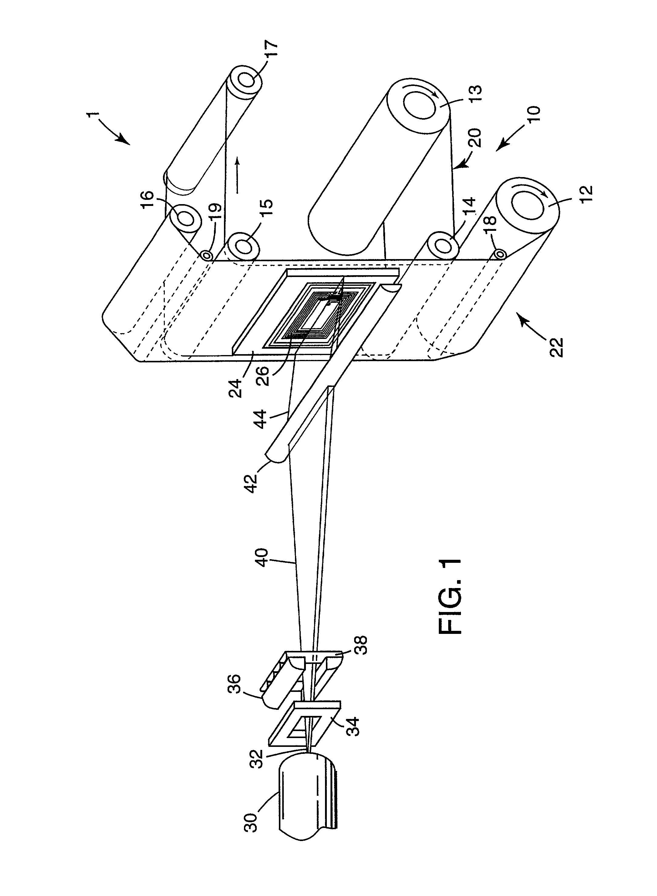
[0061] Example 4 was made in a manner similar to Example 1 except a different energy source and optical train were used, some of the conditions were changed, and a different cleaning method was used. The energy source was an infrared laser (Model 2660 Nd:YAG Infrared Laser available from Excel Technology Inc., Hauppauge, N.Y.) operating at a wavelength of 1.06 .mu.m, a repetition rate of 2000 Hz, an energy per pulse of 0.6 mJ, and a pulse width of 200 ns. The laser light incident on the metal coating was a dot or point, in contrast to the line or narrow rectangle of light in example 1 (as shown in FIG. 1). The optical trail consisted of only a round plano-convex lens with focal length of 10 cm. There was no beam shaper, homogenizer, or cylindrical lens. No mask and no protective web were used. The resulting fluence reaching the metal surface was determined from the energy output of the l...

example 5

[0063] This example illustrated the use of a metal oxide coating on the substrate.

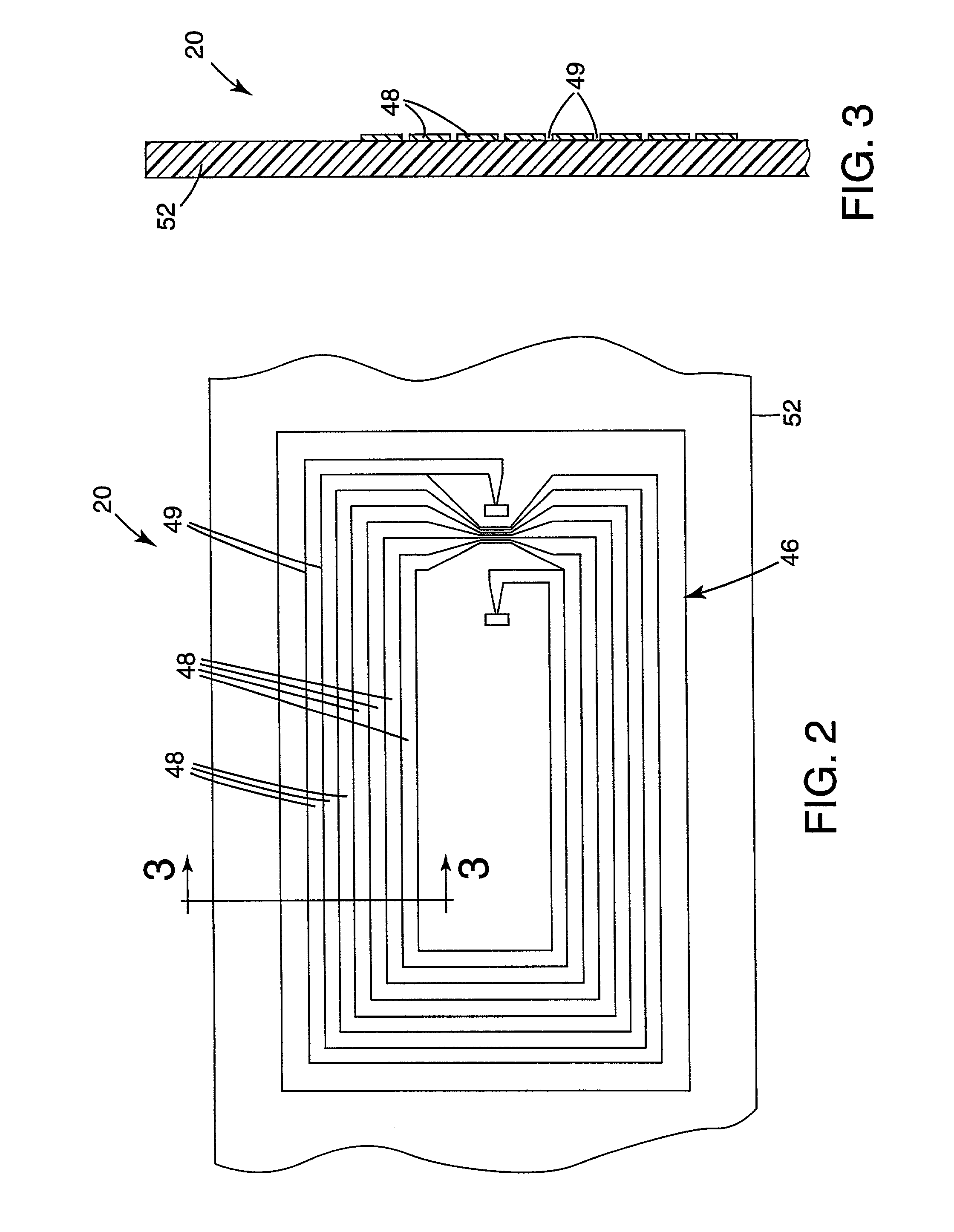
[0064] Example 3 was made as in Example 1 except that a metal oxide coated substrate was used and the energy output was reduced to about 650 mJ. The metal oxide coated substrate consisted of polyester that had been sputter coated with indium tin oxide to achieve a conductivity of 80 Ohms / square and available as No. OFC80 from Courtaulds Performance Films Inc., Canoga Park, Calif. The optical train was configured to shape the incident excimer laser beam into a 150 mm by 0.89 mm rectangle at the metal oxide surface. The energy from the excimer laser was adjusted to achieve a calculated fluence of about 80 mJ / cm.sup.2 in tills rectangle, below the ablation threshold of 90 mJ / cm.sup.2 that is needed to ablate this coating from this substrate for this wavelength. The final beam profile was overlapped by 10% for the successive pulses. The subsequent pattern had good resolution with fine features as small as ...

example 6

[0065] This example illustrated the use of a different substrate class.

[0066] Example 6 was made as in Example 1 except that a different substrate was used and the fluence was reduced. (energy level was about 650 mJ). The metal coated substrate consisted of polyimide (50 .mu.m thick film available as Kapton.TM. E from DuPont Inc., Circleville, Ohio) that had been sputter coated with copper to achieve a coating thickness of approximately 250 nm. The resulting subablation fluence used to disrupt the coating substrate interface was calculated to be 170 mJ / cm / .sup.2, below the ablation threshold of approximately 300 mJ / cm.sup.2 that is needed to ablate the metal from the substrate for this wavelength. The subsequent pattern had good resolution with fine features as small as 75 .mu.m wide lines and spaces.


PUM

PropertyMeasurementUnit
ablation threshold fluenceaaaaaaaaaa
focal lengthaaaaaaaaaa

Abstract

Patterned articles, such as RFID antenna, are made by subablation, a process comprising the steps of: A. providing a substrate having a coating, such as a metal or metal oxide, and an interface comprising the thin region where the coating and the substrate are closest to each other; B. exposing at least one part of the total area of the coating to a flux of electromagnetic energy, Such as a focused excimer laser beam, sufficient to disrupt the interface but insufficient to ablate the coating, and C. removing the parts of the coating in registry with the portion of the interface area that was disrupted, by means such as ultrasonic agitation. The process has advantages over photo-resist processes in that there is no residual chemical resist left on the product and no undercutting of the pattern or image. It has advantages over laser ablation processes in that higher throughput is possible at the same energy level and there is no microscopic debris left on the product surface.

Description

[0001] This invention relates the formation of an image or pattern in an article such as a metal coated substrate. More specifically, it relates to the formation of such an image or pattern using a high energy source such as a laser or flash lamp.[0002] Surface layer materials are often imaged or patterned for many utilitarian purposes. The surface layers may include vacuum deposited thin films, solution coatings, and electroless or electroplated films Patterned conductive surface layers may find use in both passive and active electronic circuits, display components, antennas for radio frequency identification tags (RFD), wireless local area networks (LAN), and proximity detectors as well as antennas for communication such as pagers, cell phones, and satellite reception. Optical surface layers may find application as optical components such as diffractive optical elements and security images, or in telecommunication applications as components that can perform optical switching, modu...

Claims


Application Information

Patent Timeline
Patent Type & Authority Applications(United States)
IPC IPC(8): G03F7/20B23K26/00B23K101/36B41M5/24B41M5/26G02B27/09G03F1/68G03F7/30G03F7/34H01Q1/22H01Q7/00H05K3/02
CPCB41M5/262G02B27/09G02B27/0911G02B27/0966G03F1/68G03F7/30G03F7/3014G03F7/34H01Q1/22H01Q1/2225H01Q7/00H05K3/027G02B19/009G02B19/0095G02B19/0052G02B19/0014G03F1/38G03F1/48G03F7/0025G03F7/091G03F7/70616
Inventor O'BRIEN, DENNIS P.FLORCZAK, JEFFREY M.SMITHSON, ROBERT L. W.
Owner 3M INNOVATIVE PROPERTIES CO
Why Eureka
Try Eureka