Hydrazine-free solution deposition of chalcogenide films

a technology of chalcogenide film and solution, applied in the direction of liquid/solution decomposition chemical coating, crystal growth process, coating, etc., can solve the problems of limited application of amorphous silicon, slow device speed, and the need for plasma enhanced chemical vapor deposition to achieve the effect of preparing the hydrazinium precursor more efficiently

Inactive Publication Date: 2005-01-13
GLOBALFOUNDRIES US INC
View PDF2 Cites 79 Cited by
  • Summary
  • Abstract
  • Description
  • Claims
  • Application Information

AI Technical Summary

Benefits of technology

An important advantage of the present invention results from the fact that the present invention separates the steps of forming the soluble hydrazinium based precursor from the solution processing the thin film so that a chemical company could prepare the hydrazinium precursor and the device maker could spin the films. Thus, a chemical company can prepare the hydrazinium precursor more efficiently because it is equipped to handle the toxic and reactive hydrazine and hydrazine derivatives in the plant. The device maker could then buy the precursor and spin the films according to its needs by using a less toxic solvent in its manufacturing plants.
The low-cost metal chalcogenide semiconducting materials produced according to the present invention can be used in a variety of applications, including flat panel displays, non-linear optical / photo-conductive devices, chemical sensors, emitting and charge transporting layers in light-emitting diodes, thin-film transistors, channel layers in field-effect transistors and media for optical data storage, including phase change media for optical data storage.

Problems solved by technology

Application of amorphous silicon is limited, however, to slower speed devices, since the mobility (˜10−1 cm2 / V-sec) is approximately 15,000 times smaller than that of crystalline silicon.
In addition, although amorphous silicon is cheaper to deposit than crystalline silicon, deposition of amorphous silicon still requires costly processes such as plasma enhanced chemical vapor deposition.
While very promising with regard to processing, cost, and weight considerations, organic compounds generally have a number of disadvantages, including poor thermal and mechanical stability.
In addition, while the electrical transport in organic materials has improved substantially over the last 15 years, the mobility is fundamentally limited by the weak van der Waals interactions between organic molecules (as opposed to the stronger covalent and ionic forces found in extended inorganic systems).
Metal halides are relatively ionic in nature, thereby limiting the selection of possible semiconducting systems with potential for high mobility.
In addition, the tin(II)-iodide-based systems in particular are highly air sensitive and all processing must by done under inert-amosphere conditions.
While the potential for higher mobility exists, the increased covalency of the extended metal chalcogenide systems also reduces their solubility and increases the melting temperature, rendering simple and low-cost thin-film deposition techniques for these systems a significant challenge.
However, these techniques are generally not amenable to low-cost, high-thoughput (fast) solution-based deposition techniques such as spin-coating, printing and stamping.
While metal chalcogenide films are formed using this technique, the films generally have substantial impurities of halogen, carbon or nitrogen.
Annealing in reducing atmospheres of H2 or H2S at temperatures up to 450° C. can be used to reduce the level of impurities in the film, but these relatively aggressive treatments are not compatible with a wide range of substrate materials and / or require specialized equipment.
Further, reported TFT devices prepared using this technique exhibited unusual features, including substantial device hysteresis and a negative resistance in the saturation regime, perhaps as a result of trap or interface states either within the semiconducting film or at the interface between the semiconductor and the insulator.
However, in this process, the species used to solublize the chalcogenide framework (i.e., quaternary ammonium or phosphonium polyselenides), which ultimately decompose from the sample during the heat treatment, are very bulky and most of the film disappears during the annealing sequence (e.g., 70-87%).
The resulting films consequently exhibit inferior connectivity and quality.
), making this process incompatible with even the most thermally robust plastic substrates (e.g., Kapton sheet can withstand temperatures as high as 400° C.).
), rendering the process incompatible with organic-based flexible substrate materials.
53, 6979-6982 (1982)], but attempts to deposit other main-group metal chalcogenides, such as Sb2S3 and GeSx have not been successful, due to the low solubility of the precursors in the diamine solvents [J. Putz and M. A. Aegerter, “Spin-Coating of MoS2 Thin Films,” Proc. of International Congress on Glass, vol.
While this process enables the deposition of high quality ultrathin spin-coated films with field-effect mobilities as high as 10 cm2N-sec, approximately an order of magnitude higher than previous examples of spin-coated semiconductors, the process has the disadvantage that it requires spinning the film from a solution containing hydrazine, which is a highly toxic and reactive substance.

Method used


Image

  • Hydrazine-free solution deposition of chalcogenide films
  • Hydrazine-free solution deposition of chalcogenide films
  • Hydrazine-free solution deposition of chalcogenide films

Examples


example 1

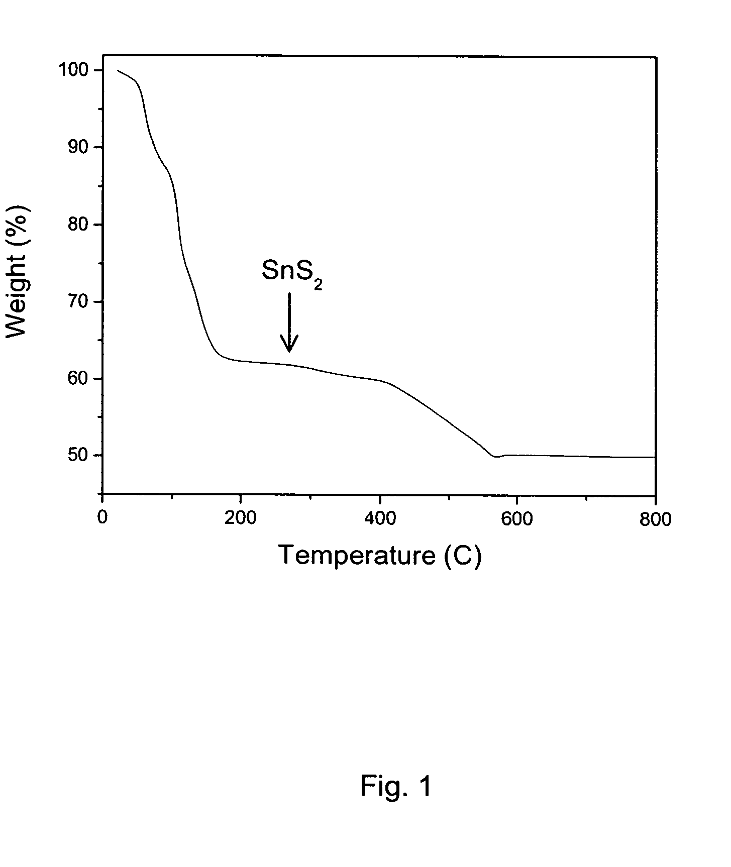
A solution of SnS2 was formed by dissolving 0.274 g SnS2 (1.5 mmol) in 1.0 ml hydrazine and 0.048 g sulfur (1.5 mmol). Substantial bubbling is observed during the dissolution process, presumably as a result of evolution of primarily nitrogen during the reaction. The dissolution is somewhat slow at room temperature, requiring approximately 4-6 hours of stirring to produce a clear yellow solution. The solution was filtered and the filtrate was evaporated under a flow of nitrogen gas, ultimately yielding 0.337 g of yellow powder. Thermal analysis of the powder indicates that the resulting solid decomposes to form SnS2 at a relatively low temperature, essentially by 200° C., with a weight loss of 38% observed during the process (FIG. 1).

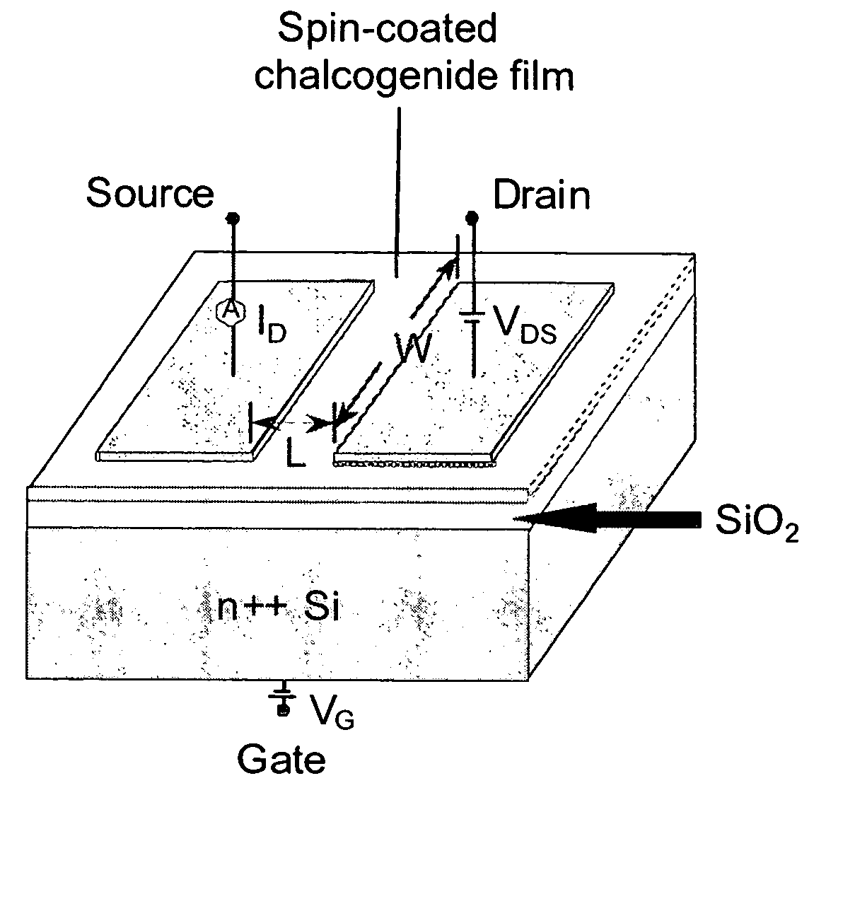
A film of the above-described precursor can readily be deposited on a cleaned quartz substrate by dissolving 0.055 g SnS2 (0.3 mmol) in 0.5 ml hydrazine and 0.010 g sulfur (0.3 mmol). Each substrate was precleaned sequentially in aqua regia, toluene, ...

example 2

SnSe2 films were also deposited using the above-described technique.

0.277 g SnSe2 (1 mmol) was readily dissolved (in several minutes, with stirring) in 1 ml hydrazine when 0.079 g Se (1 mmol) have been added, yielding ultimately a light yellow solution. The light yellow coloration suggests the lack of formation of polychalcogenides during the process although if larger quantities of Se are added, a darker coloration of the solution is observed. Substantial bubbling is observed during the dissolution process, presumably as a result of evolution of primarily nitrogen during the reaction. Evaporating the solution under flowing nitrogen gas over the period of several hours leads to the formation of approximately 0.450 g of a yellow crystalline powder. The powder rapidly loses weight while sitting on a balance at room temperature, suggesting incorporation of solvent (i.e., hydrazine) within the structure, which slowly dissociates from the sample.

Single crystal structure refinement o...

example 3

In this example, the ammonium-based tin(IV) sulfide precursor was synthesized by dissolving 548.5 mg of SnS2 (3 mmol) in 85 ml of 50 wt. % aqueous ammonium sulfide, (NH4)2S, over a period of 4 days. The solution was filtered through a 0.45 μm glass microfiber filter and the resulting filtered solution was slowly evaporated under a flow of nitrogen gas over a period of several days, leading to a yellow product (˜1.05 g).

The product was repeatedly washed / filtered with methanol until the resulting filtrate was colorless and the thermal analysis scan on the final product yields a weight-loss transition at −150° C. (to yield SnS2) of approximately 30% (FIG. 5). This indicates an approximate composition, (NH4)2SnS3. The product is nominally amorphous, i.e., no X-ray pattern is observed in a powder diffractometer. The weight loss, which corresponds to loss of ammonia and hydrogen sulfide, is initiated at temperatures as low as ambient temperature, indicating the ease with which the mate...


PUM

PropertyMeasurementUnit
temperatureaaaaaaaaaa
temperaturesaaaaaaaaaa

Abstract

A method of depositing a film of a metal chalcogenide including the steps of: contacting an isolated hydrazinium-based precursor of a metal chalcogenide and a solvent having therein a solubilizing additive to form a solution of a complex thereof; applying the solution of the complex onto a substrate to produce a coating of the solution on the substrate; removing the solvent from the coating to produce a film of the complex on the substrate; and thereafter annealing the film of the complex to produce a metal chalcogenide film on the substrate. Also provided is a process for preparing an isolated hydrazinium-based precursor of a metal chalcogenide as well as a thin-film field-effect transistor device using the metal chalcogenides as the channel layer.

Description

BACKGROUND OF THE INVENTION 1. Field of the Invention The present invention relates to methods of depositing a film of a metal chalcogenide from hydrazine-free solutions and a method of preparing a field-effect transistor including a film of a metal chalcogenide deposited from hydrazine-free solutions. More particularly, the present invention relates to a method of preparing a field-effect transistor including as the channel layer a film of a metal chalcogenide deposited from hydrazine-free solutions. 2. Description of the Prior Art The ability to deposit high quality semiconducting, metallic and insulating thin films forms one of the important pillars of present-day solid-state electronics. A solar cell may include, for example, a thin n-type semiconductor layer (˜0.25 μm) deposited on a p-type substrate, with electrical contacts attached to each layer to collect the photocurrent. Light-emitting diodes (LED's) are typically comprised of a p-n bilayer, which under proper forward...

Claims


Application Information

Patent Timeline
Patent Type & Authority Applications(United States)
IPC IPC(8): H01L21/368C23C18/12C23C22/02C30B1/02H01L21/336H01L29/786H01L31/18
CPCC23C18/1204H01L29/78681H01L29/66742H01L21/02568H01L21/02628C23C22/02C30B1/02H01L31/18
Inventor MITZI, DAVID B.COPEL, MATTHEW W.
Owner GLOBALFOUNDRIES US INC
Why Eureka
Try Eureka