Low voltage electron source with self aligned gate apertures, fabrication method thereof, and luminous display using the electron source

a low-voltage electron source and gate aperture technology, which is applied in the manufacture of electrode systems, electric discharge tubes/lamps, and screens for tubes, etc., can solve the problems of device drivers, current state of the art of cnt electron sources that do not meet the above requirements, and have not found any product applications

Inactive Publication Date: 2005-06-16
TOLT ZHIDAN LI
View PDF51 Cites 96 Cited by
  • Summary
  • Abstract
  • Description
  • Claims
  • Application Information

AI Technical Summary

Benefits of technology

[0016] It is the objective of the current invention to: a) provide a method to fabricate a self-aligned gate aperture with a diameter on the order of 100 nanometer around each vertically oriented CNT and with equal distance to each CNT; b) provide a method for controlling CNT growth over large area so that they are mono-dispersed, with a

Problems solved by technology

The cost of a device driver, which often is a major cost component, power consumption, as well as device miniaturization are all depend on the modulation voltage.
Despite the superior emission properties of a single CNT, the current state of the art of a CNT electron source does not meet most of the above requirements and, therefore, has not found any product applications yet, despite the appearance of some prototype flat panel displays.
Both methods are difficult to implement in production.
E-beam lithography is so slow and expensive that it is ill suited for any meaningful operation.
Applying a mono-layer consistently over large an area is no easy task.
b) Difficulty in Fabrication of an Integrated Gate Structure
Two obstacles make the fabrication difficult.
First, CNT films is sensitive to wet processes.
Upon exposure to a wet agent, CNTs either stick to the substrate or to themselves, diminishing their field emission properties.
The problem is that a group of densely grown CNTs in a single gate hole does not emit

Method used


Image

  • Low voltage electron source with self aligned gate apertures, fabrication method thereof, and luminous display using the electron source
  • Low voltage electron source with self aligned gate apertures, fabrication method thereof, and luminous display using the electron source
  • Low voltage electron source with self aligned gate apertures, fabrication method thereof, and luminous display using the electron source

Examples


Embodiment Construction

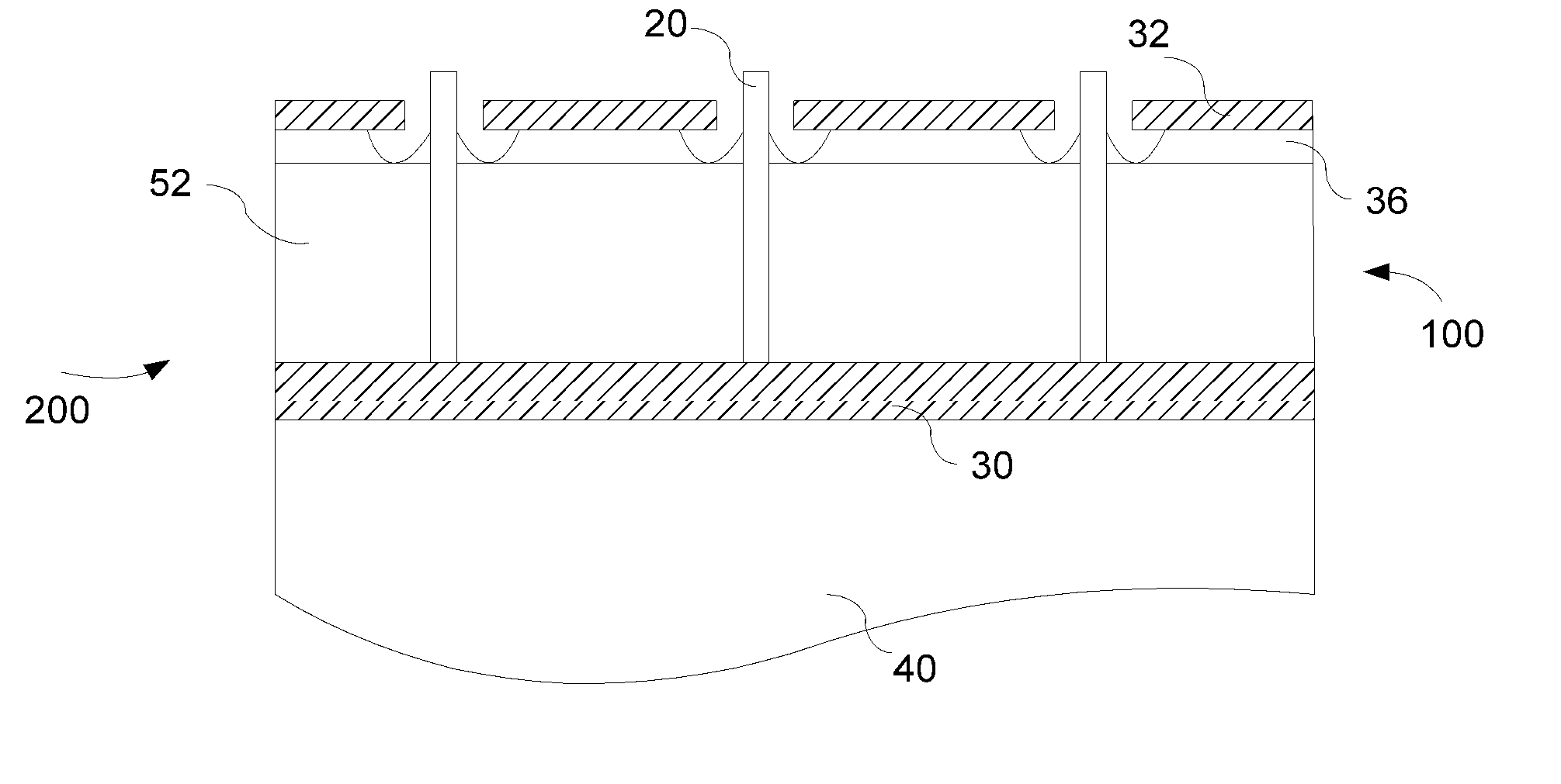
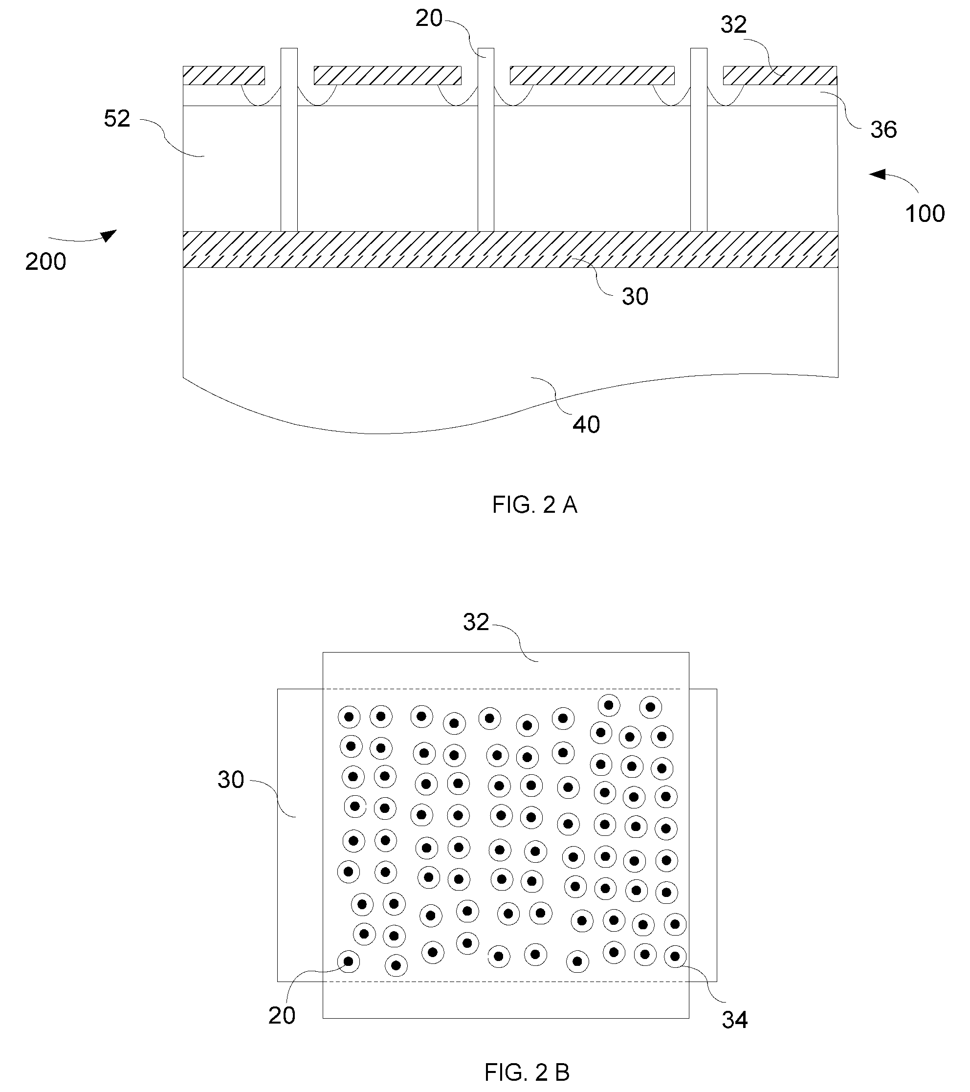
[0059]FIG. 2 illustrates an electron source 200 by current invention using vertically aligned and mono-dispersed CNT 20 as emitter. It includes a cathode electrode 30 deposited on a substrate 40; an emitter layer 100 disposed over the cathode and formed from an embedding dielectric 52 and an array of CNTs embedded therein, the emitter layer having a surface parallel to which the CNTs have been truncated to the same length, and above the surface the CNTs protrude by a small fraction of one micrometer; a gate insulator 36 disposed over the emitter layer of a thickness on the order of 100 nm and having an array of apertures, each aligned with and exposes one nano-structure in the emitter layer; and a gate electrode 32 deposited on the gate insulator and having an array of apertures 34 aligned with the apertures in the insulator and spaced from the exposed CNT by approximately the thickness of the insulator. When a positive voltage is applied between the gate and the cathode electrodes,...


PUM


Abstract

An electron source include a first cathode electrode disposed over a substrate and terminated to provide electrons; an emitter layer disposed over the cathode electrode and formed from one or plurality vertically aligned and mono-dispersed nano-structures that are truncated to the same length, embedded in a solid matrix and protruding above the surface for emitting electrons; an insulator disposed over the emitter layer and having one or plurality of apertures, each is self-aligned with and exposes one nano-structure in the emitter layer; and a second gate electrode disposed over the insulator, having one or plurality of apertures self-aligned with the apertures in the insulator and terminated to extract electrons from the exposed nano-structures through the apertures. The gate aperture is substantially less than one micrometer and the gated nano-structures can have a density on the order of 108/cm2. Such an electron source can be modulated with an extra low voltage, emits electrons with high current density and high uniformity, and operates with high energy-efficiency and long lifetime.

Description

BACKGROUND OF INVENTION [0001] The present invention relates to an emission electron source using nano-structures as emitters and self-aligned and nano-sized gate aperture for low voltage control, the fabrication method thereof and its use in flat panel display. [0002] There has been broad interest in the field emission application of nano-structured materials because of their inherited high aspect ratio. Among various materials, Carbon nano-tube (CNT) appears the most promising. Numerous studies have reported the advantageous emission properties of CNT. It has a threshold field as low as 1 to 2×10⁶ V / m, a low electron energy spread, and can carry a current as high as 500 nA (nano-Amperes) per tube. Its extraordinary high electrical and thermal conductivity as well as strong chemical and mechanical stability make it an ideal field emitter. [0003] Potential applications of a CNT field emission device include flat panel displays, 2D sensors, direct writing e-beam lithography, microwav...

Claims


Application Information

Patent Timeline
IPC IPC(8): H01J3/02H01J9/02H01J31/12
CPCB82Y10/00H01J3/022H01J2201/30469H01J31/127H01J9/025
Inventor TOLT, ZHIDAN LI
Owner TOLT ZHIDAN LI
Why Eureka
Try Eureka