Laser diode and manufacturing method thereof

Active Publication Date: 2005-06-16
LUMENTUM JAPAN INC
View PDF1 Cites 71 Cited by
  • Summary
  • Abstract
  • Description
  • Claims
  • Application Information

AI Technical Summary

Benefits of technology

[0014] Various studies have been found that in a case where the oxygen composition of aluminum oxide is 10% or less of the stoichiometric composition, that is, in a case of: Al2O3-x (X≦0.3) in the chemical formula lowering of resistance to damp caused by oxygen defects in the film, an increase in the absorption of light and an increase of the number of surface states caused at the interface of semiconductor and aluminum oxide due to defects are each at a negligible level, and cause no undesired effects on the device characteristics. FIG. 11 shows occurrence of film peeling-off after keeping for 300 hours under the conditions of a temperature of 85° C. and a humidity of 85%. As apparent from the graph, film peeling-off did not occur in a case where X≦0.3. FIG. 12 shows the dependence of an extinction coefficient of an aluminum oxide film on the oxygen concentration. The extinction coefficient shows the extent of light absorption, and the light absorption did not occur in a case where X≦0.2, and light absorption caused no practical problem even at X=0.3. FIG. 13 shows the dependence of critical load on the oxygen concentration in a scratch test. The critical load is a load at which film peeling-off starts in the scratch test, which is an index for adhesion. It was found that, in an aluminum oxide film with no oxygen defects, the film was scarcely adhered and highly liable to be peeled off. The adhesion is improved in the loss of oxygen state and it can be seen that adhesion is improved in the loss of oxygen state, and a preferred film has the highest adhesion at X=0.2. The adhesion is rather lowered when the loss of oxygen component increases more. In view of experience, there is no practical problem in a case where the critical load is 30 mN or more. FIG. 14 shows a surface state density at an interface of InP and aluminum oxide film obtained by measurement for characteristics of high frequency capacitance/voltage characteristics. At X=0.2 or less, the surface states density is less than the detectable limit and the amount thereof is slight also at X=0.3. As described above, it has been found that favorable characteristics with no practical problems at all are shown at X≦0.3 as described above. In particular, in a case where Al2O3-x (X≦0.2), each of lowering in the resistance to damp, increase in the light absorption and increase of the surface states density is less than the detectable limit and it is extremely satisfactory. Further, for the spontaneous oxide film formed at the facet by contact with atmospheric air after the formation of the facet by cleavage or the like, oxygen is absorbed in aluminum oxide by the formation of aluminum oxide in the state of lacking in oxygen, to obtain a clean interface of semiconductor and aluminum oxide. It is probably that this improved adhesion between the reflection film and the semiconductor as shown in FIG. 13.
[0015] Since diffusion of oxygen to the semiconductor can be suppressed and bonding of semiconductor-constituting elements, particularly, aluminum and arsenic with oxygen can be prevented by forming the state of lacking in oxygen, facet deterioration can be minimized. FIG. 15 shows a result of conducting an automatic power controlled operation test at a temperature of 85° C. and then allowing an operation current to flow till the laser diode emits the maximum optical power and examining whether catastrophic optical damages are caused or not. The catastrophic optical damages were not caused in X≧0.03 (as shown by symbols “◯” in FIG. 15, catastrophic optical damage was not caused in the continuous operation test till 5000 hours). FIG. 16 shows a result of conducting an automatic power controlled operation test for 100 hours, then applying a pulsative DC voltage and examining a voltage causing electrostatic destroy deterioration. The electrostatic destroy deterioration was no more caused in X≧0.03 and at 500 V or lower and, particularly, deterioration was no more caused upon application of a voltage even at 1000 V in X≧0.1 (symbol “◯” shown in FIG. 16). As described above in a case where loss of oxygen of at least 1% or more relative to the stoichiometric composition is present, that is, at Al2O3-x (0.03≦X), the effects for minimizing

Problems solved by technology

However, since the nitride film such as a silicon nitride film has a large internal stress, it may cause undesired effects on the reliability due to the increase of the total stress of the ref

Method used


Image

  • Laser diode and manufacturing method thereof
  • Laser diode and manufacturing method thereof
  • Laser diode and manufacturing method thereof

Examples


Example

EXAMPLE 1

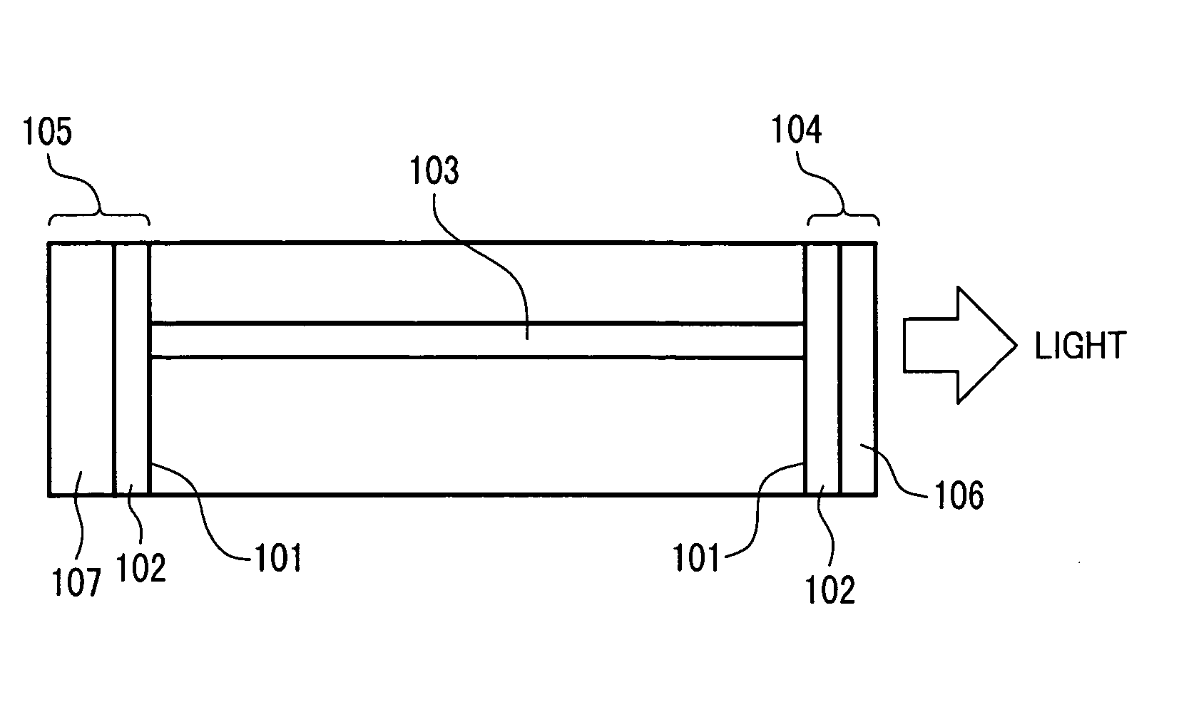
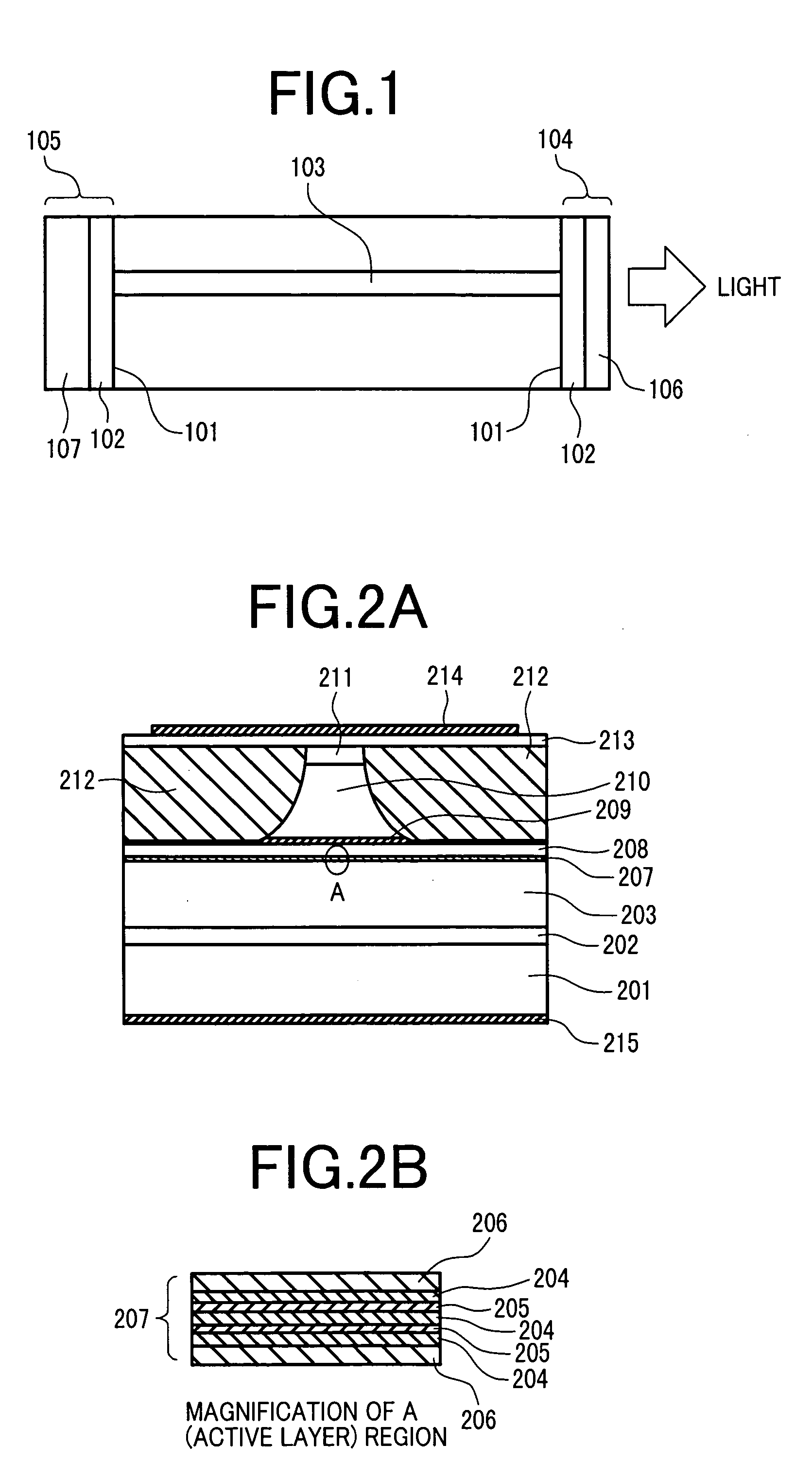
[0038] A first example of the invention is to be explained with reference to FIGS. 2A, 2B and 3. This example is applied to a high power laser diode for 0.65 μm band used for writing in optical disks or magneto-optical disks. FIG. 2A shows a cross-sectional structure, FIG. 2B is an enlarged view of an active layer, and FIG. 3 shows planer structure. Then a device manufacturing method is to be described. On an n-typed GaAs substrate 201, are formed successively, a GaAs buffer layer 202, an n-typed (AlxGa1-x)InP clad layer 203 lattice matched to GaAs (x=0.7), a strained quantum well active layer 207 comprising (AlyGa1-y)InP barrier layers (y=0.45, barrier layer thickness 4 nm) 204 lattice matched to GaAs, InzGa1-zP strained quantum well layers (z ˜0.58, well layer thickness 87 nm) 205, and (AlsGa1-s)Inp SCH (Separate Confinement Heterostructure) layers (s=0.55, barrier wall layer thickness 4 nm) 206, a p-typed (AltGa1-t)InP clad layer (t=0.7) 208 lattice matched to GaAs, a p...

Example

EXAMPLE 2

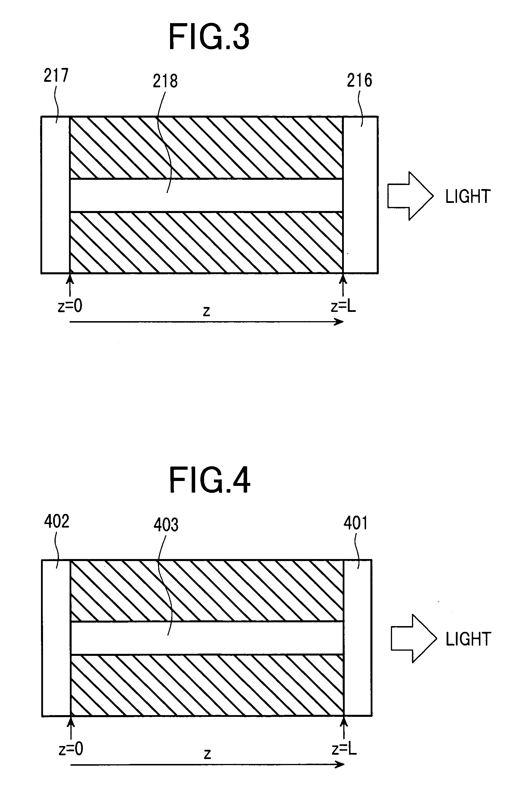
[0041] A second example of the invention is to be described with reference to FIGS. 4, 5A and 5B. In this example, the invention is applied to a high power laser diode for 0.98 μm band for a rare earth-doped optical fiber amplifier excitation for use in relays or receivers in optical transmitting systems. FIG. 4 shows a planar structure of a laser diode having a Fabry-Pelot type optical resonator, FIG. 5A shows a cross-sectional structure of the same and FIG. 5B shows an enlarged view of an active layer. Then, a device manufacturing method is to be described. On an n-typed GaAs substrate 501, are formed successively, a GaAs buffer layer 502, an n-typed InGaP clad layer 503 latticed matched to GaAs, a strained quantum well active layer 506 comprising In1-xGaxAsyP1-y barrier layers (x=0.82, y=0.63, a barrier layer thickness 35 nm) 504 lattice matched to GaAs, and an InxGa1-zAs strained quantum well layer (z 0.16, well layer thickness 7 mm) 505, a p-typed InGaP clad layer 507...

Example

EXAMPLE 3

[0043] A third example applying the invention is to be explained with reference to FIGS. 6 and 7. In this example, the invention is applied to a laser diode for 1.3 μm band used as a light source in subscriber's optical transmission systems. FIG. 6 is a perspective structure of a laser diode and FIG. 7 shows a cross sectional structure. Then, a device manufacturing method is to be described. After growing an n-typed InP buffer layer 702 on an n-typed InP substrate 601, 701, an n-typed InAlAs clad layer 703 lattice matched to InP, an n-typed InGaAlAs lower SCH layer 704, a strained quantum well active layer 705 comprising an InGaAlAs strained barrier layer (band gap: 1.32 eV, barrier layer thickness: 8 nm) and an InGaAlAs strained quantum well layer. (band gap: 0.87 eV, well layer thickness: 6 nm), a p-typed InGaAlAs upper SCH layer 706 lattice matched to the InP substrate, a p-typed InAlAs first clad layer 707, a p-typed InP second clad layer 708, a p-typed InGaAs cap laye...


PUM


Abstract

Laser diodes containing aluminum at high concentration in an active layer have been usually suffered from remarkable facet deterioration along with laser driving operation and it has been difficult for the laser diodes to attain high reliability. An aluminum oxide film lacking in oxygen is formed adjacent to the semiconductor on an optical resonator facet, by which facet deterioration can be minimized and, accordingly, the laser diode can be operated with no facet deterioration at high temperature for long time and a laser diode of high reliability can be manufactured at a reduced cost.

Description

BACKGROUND OF THE INVENTION [0001] 1. Field of the Invention [0002] The present invention relates to a semiconductor light source typically represented by a laser diode and, more in particular, it relates to a semiconductor light source suitable for use in writing light sources of optical disks or magneto-optical disks, and for use in optical communication modules, optical communication systems, and optical networks. [0003] 2. Description of the Related Art [0004] At present, laser diodes with a high degree of reliability have been demanded for use in writing to optical disks or magneto-optical disks, as well as in optical communication systems. Such laser diodes are required to operate for a long time, stably in a basic mode. A coating film made of an insulator film is applied to the surface of a semiconductor forming a light emission surface of semiconductor laser diodes. This is used to improve the light outputting efficiency by obtaining an appropriate reflectivity and to preven...

Claims


Application Information

Patent Timeline
IPC IPC(8): B82Y20/00H01L21/00H01S5/028H01S5/0683H01S5/12H01S5/223H01S5/227
CPCH01S5/0014H01S5/02216H01S5/02284H01S5/0282H01S5/227H01S5/1039H01S5/12H01S5/2231H01S5/0683H01L2224/48091H01L2224/45144H01S5/02251H01L2924/00014H01L2924/00
Inventor KIKAWA, TAKESHINAKAHARA, KOUJINOMOTO, ETSUKO
Owner LUMENTUM JAPAN INC
Why Eureka
Try Eureka