Materials for electroluminescent devices

a technology of electroluminescent devices and materials, applied in the direction of luminescnet screens, discharge tubes, natural mineral layered products, etc., can solve the problems of no blue emission from fluorescent or phosphorescent emitters, and only achieve full color displays, so as to improve efficiency and reduce driving voltage , the effect of increasing the efficiency

Active Publication Date: 2005-07-14
VERSITECH LTD
View PDF9 Cites 14 Cited by
  • Summary
  • Abstract
  • Description
  • Claims
  • Application Information

AI Technical Summary

Benefits of technology

[0009] The invention also provides an EL device of enhanced performance, including but not limited to, purer color achievement, higher efficiency and lower driving voltage. Therefore, this invention is also directed to the application of the aforesaid materials in EL devices, in particular OLEDs and PLEDs. The employment of these materials can be in any, or one or more of the following layers of the devices: hole-injection layer, hole-transporting layer, electron-injection layer, electron-transporting layer, emissive layer comprising of a single emitter or host for one or more emissive dopant(s), hole-blocking layer and/or electron-blocking layer, and the like, but is not limited to the above examples. In the devices, thin films of the materials based on formula I alone or the materials based o...

Problems solved by technology

Emission from non-targeted species present in the device, especially the host, is another obstacle to overcome before high color purity can be obtained; and full color displays can only be achieved when the colors can be cont...

Method used


Image

  • Materials for electroluminescent devices
  • Materials for electroluminescent devices
  • Materials for electroluminescent devices

Examples


example 1

Preparation of Compound 2

[0080] Freshly distilled aniline (5 g, 0.055 mole) was introduced into a round-bottom flask containing borane triethylamine compound (9 mL, 0.061 mole) under an argon atmosphere. The mixture was heated to 80° C. for 16 hours, and then further to 180° C. Afterwards, the excess reactant was removed in vacuo. The product was collected upon cooling the reaction mixture to room temperature, and then purified using high vacuum sublimation. White solid (3 g, 53% yield) was obtained. 1H NMR (300 MHz, CDCl3) δ 7.35 (t, J=6.90 Hz, 6H), 7.25-7.18 (m, 9H), 5.00 (bs, 3H) (notes: t=triplet, m=multiplet, b=broad, s=singlet). 13C NMR (75 MHz, CDCl3,) δ 148.0, 128.8, 125.2, 124.7. FAB-MS(m / z): 309 [M+]. M. P. 167° C. (DSC). Tg: 121° C. Td: 203° C.

example 2

Preparation of Compound 3

[0081] Freshly distilled acetonitrile (2 g, 0.048 mole) was introduced into a round-bottom flask containing calcium chloride-dried chlorobenzene under an argon atmosphere. Boron trichloride gas was then continuously bubbled into the solution until fuming is observed above the flask neck, indicating that all acetronitrile was consumed. Dried ammonium chloride powder (2.8 g) was added and the reaction mixture was refluxed for 3 hours. Upon cooling the reaction mixture to room temperature, the chlorobenzene was removed using a cannula. This was followed by the introduction of 150 mL benzene into the reaction mass, and after that the addition of 100 mL a benzene solution of the 15 g (0.088 mole) diphenylamine dropwise to the reaction mixture. The reaction mixture was then refluxed for 16 hours. The white product (4.5 g, 48% yield) was collected with filtration and purified using high vacuum sublimation. FAB-MS(m / z): 582 [M+]. Anal. Calculated for C36H33B3N6: C,...

example 3

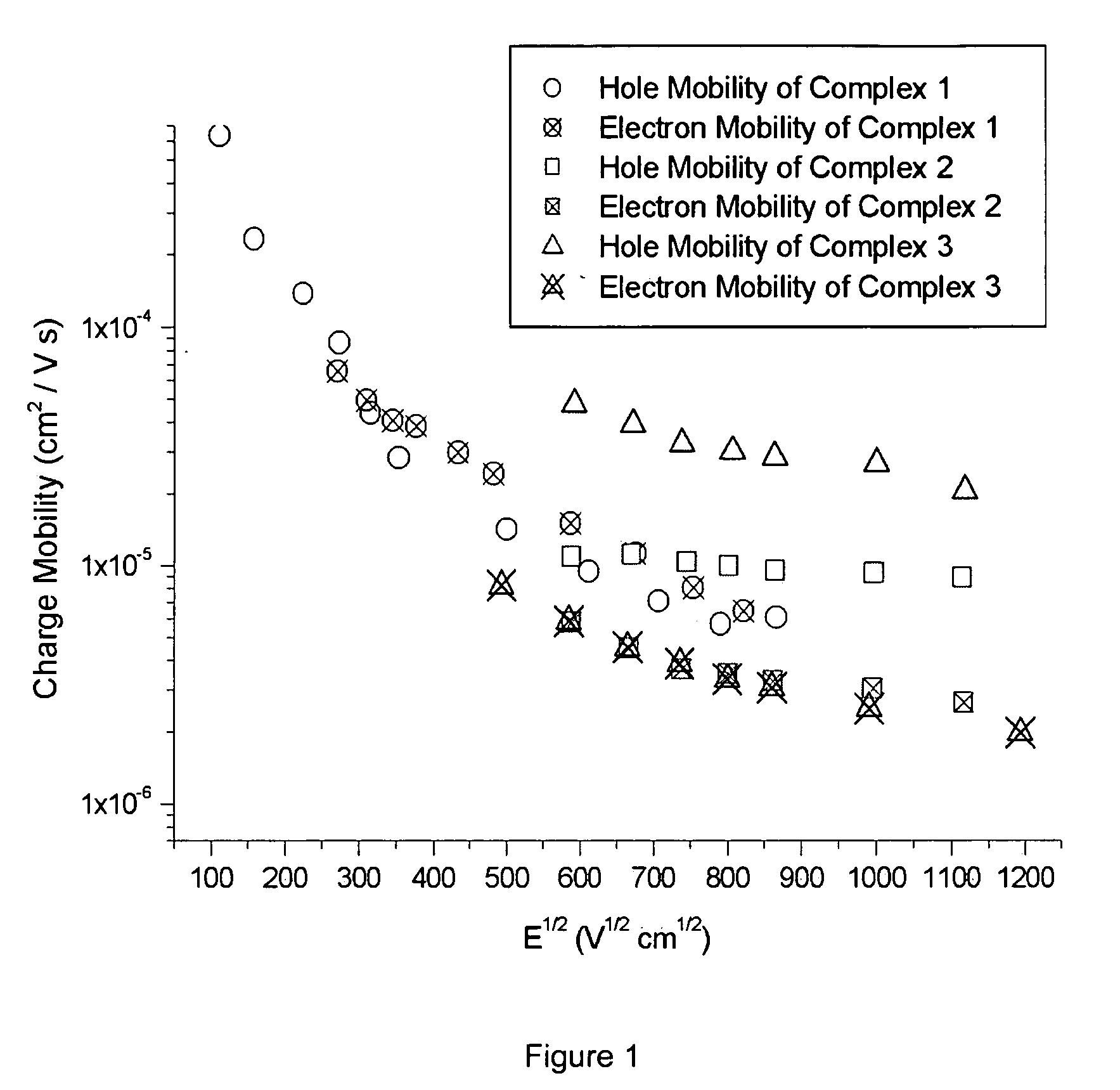
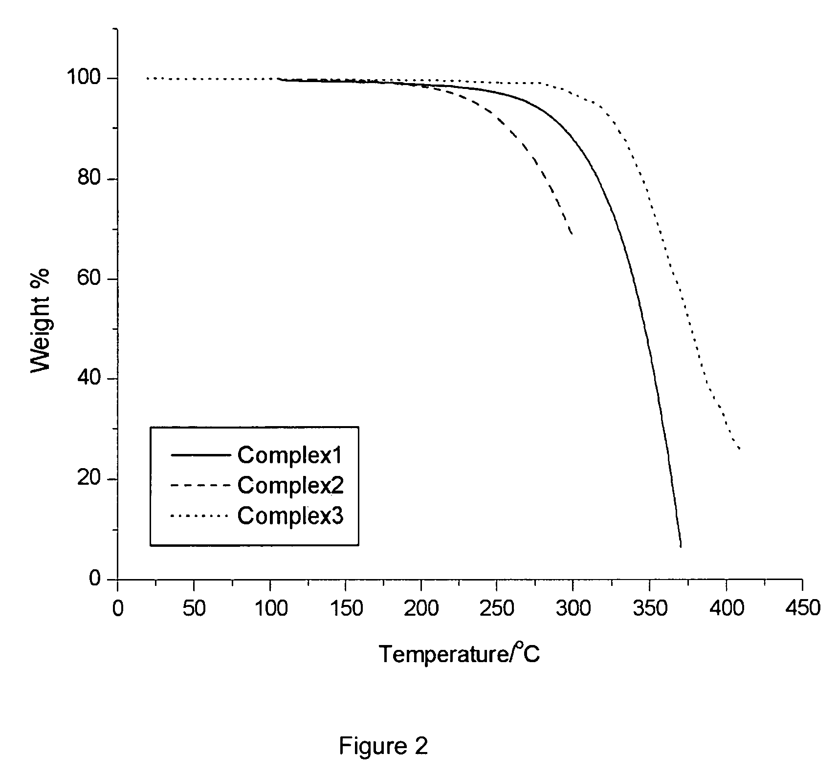
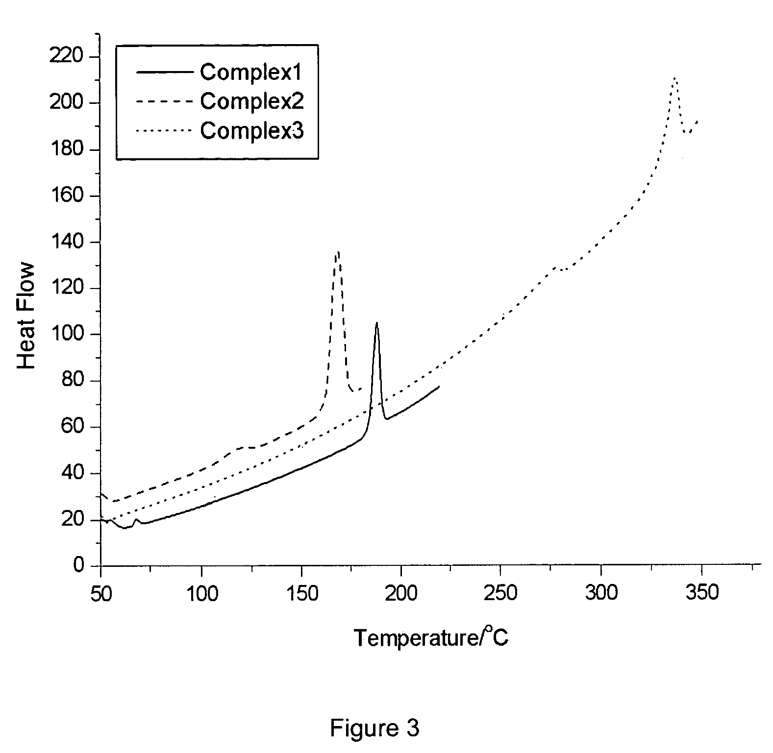
[0082] The physical parameters for Compounds 1, 2 and 3 were determined and are summarized in Table 1.

PhysicalCompoundCompoundCompoundParameters123Hole Mobility (cm2 / V · s)up to 10−4up to 10−5up to 1O−5Electron Mobility (cm2 / V · s)up to 10−5up to 10−6up to 10−5Decomposition Temperature227203287(Td, ° C.)Glass Transition Temperature68112278(Tg, ° C.)HOMO (eV)−5.3−5.3*LUMO (eV)−1.0−0.8*Absorption λmax264231* (nm) in DMF solutionEmission λmax288n.o.* (nm) in DMF solution

* = no measurement was made.

n.o. = not observed


PUM

PropertyMeasurementUnit
Electron mobilityaaaaaaaaaa
Electroluminescenceaaaaaaaaaa
Aromaticityaaaaaaaaaa

Abstract

Materials containing one or more borazine rings are employed as materials for electroluminescent devices. The compounds have molecular structures represented by the following formula:
in which R1—R6 are independently a metal; a whole or part of an optionally substituted borazine ring; hydrogen; halogen; hydroxyl; optionally substituted alkyl, cycloalkyl, aryl, acyl, alkoxy, acyloxy, amino, acylamino, aralkyl, cyano, carboxyl, thio, vinyl, styryl, aminocarbonyl, carbamoyl, aryloxycarbonyl, phenoxycarbonyl, or alkoxycarbonyl, as well as recognized donor and acceptor groups. The compounds have high thermal stability as well as hole and electron mobilities.

Description

FIELD OF THE INVENTION [0001] The present invention relates to novel electroluminescent (EL) devices, including organic and polymer light-emitting devices (OLEDs and PLEDs), which are capable of emitting light in the UV or the visible regions. More particularly, this invention relates to the employment of borazine-containing materials in one or more layers of EL devices, OLEDs and PLEDs. Such layers include the hole-injection layer, hole-transporting layer, electron-injection layer, electron-transporting layer, emissive layer comprising of a single emitter or host with one or more emissive dopant(s) hole-blocking layer and / or electron-blocking layer and the like, but are not limited to these examples. The application of the aforesaid materials in EL devices can enhance the device performance, including but not limited to, the achievement of purer color, higher efficiency and lower driving voltage. Further, the present invention relates to the processes for effectively preparing the ...

Claims


Application Information

Patent Timeline
IPC IPC(8): C07F5/02C07F5/05C09K11/06H05B33/14H05B33/20
CPCC07F5/022C09K11/06Y10S428/917H05B33/14C09K2211/1085
Inventor CHE, CHI-MINGSHAM, IONA HIU TUNG
Owner VERSITECH LTD
Why Eureka
Try Eureka