Method for doping impurities, methods for producing semiconductor device and applied electronic apparatus

a technology of electronic equipment and impurities, applied in the direction of excavating, foundation engineering, transistors, etc., can solve the problems of increasing the temperature of the substrate, hardly using glass substrates with relatively low melting points for such processes, and the inability of ion implantation to apply to plastic substrates with low melting points. , to achieve the effect of reducing the amount of dopants used, reducing the burden on the human body and the environment, and reducing the contamination of the apparatus level level

Inactive Publication Date: 2005-08-18
SONY CORP
View PDF7 Cites 173 Cited by
  • Summary
  • Abstract
  • Description
  • Claims
  • Application Information

AI Technical Summary

Benefits of technology

[0014] Accordingly, it is an object of the present invention to provide a method for doping impurities, methods for producing a semiconductor device and an applied electronic apparatus employing the process. The method for doping impurities has the following advantages: no need to use toxic impuri

Problems solved by technology

That is, glass substrates that have relatively low melting points are hardly used for such processes.
This ion implantation has the following disadvantages: The temperature of a substrate is increased because of the energy of the implanted ions; thus, the ion implantation cannot be applicable to a plastic substrate having a low melting point.
In view of employing a beam scan and the size of apparatus, the ion implantation is not suitable for a large-area process.
However, a semiconductor film subjected to ion doping or plasma doping contains a large amount of hydrogen.
However, the plastic substrate cannot be heated to a temperature required for removing hydrogen (400° C. to 460° C.).
As a result, subse

Method used


Image

  • Method for doping impurities, methods for producing semiconductor device and applied electronic apparatus
  • Method for doping impurities, methods for producing semiconductor device and applied electronic apparatus
  • Method for doping impurities, methods for producing semiconductor device and applied electronic apparatus

Examples


example 1

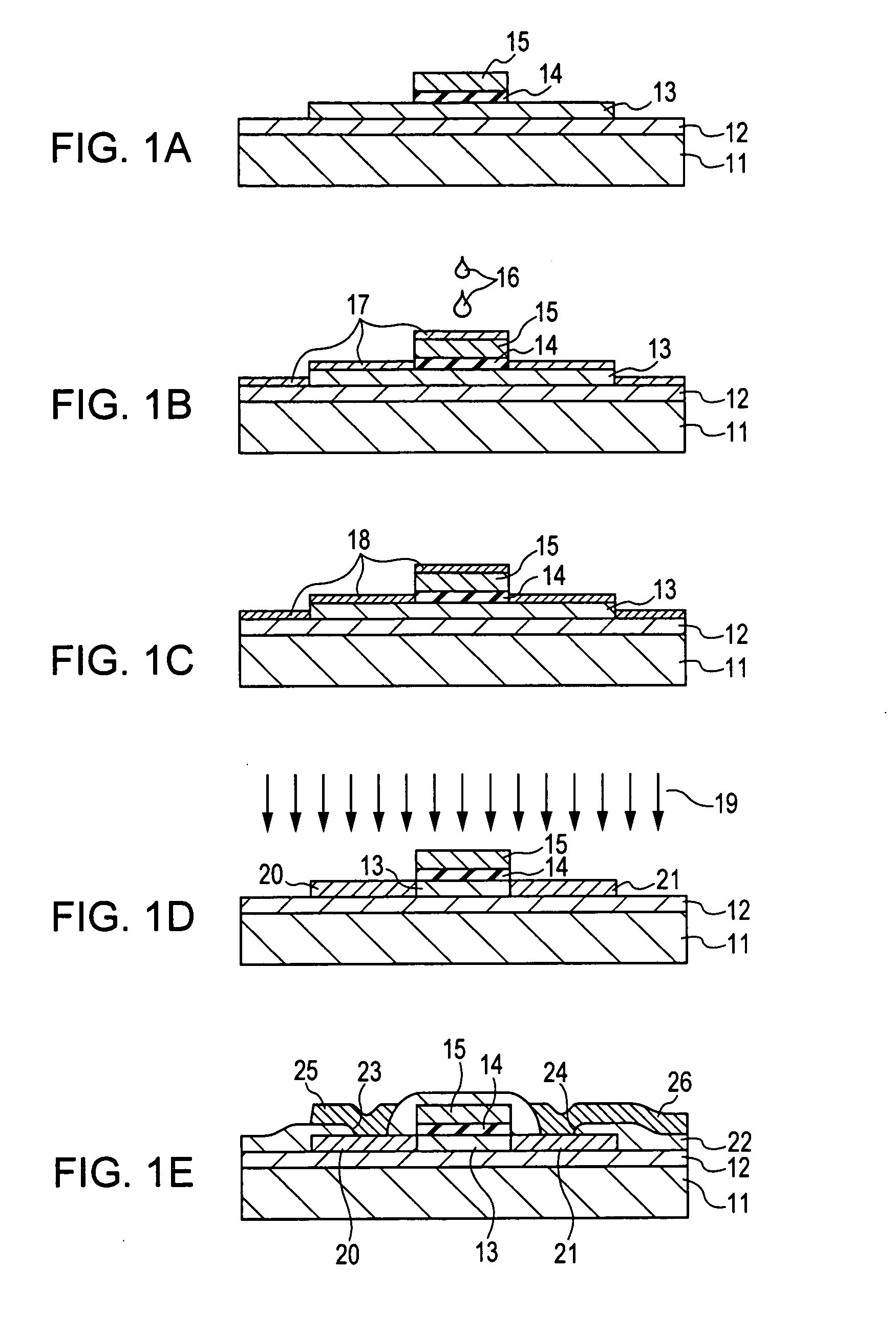
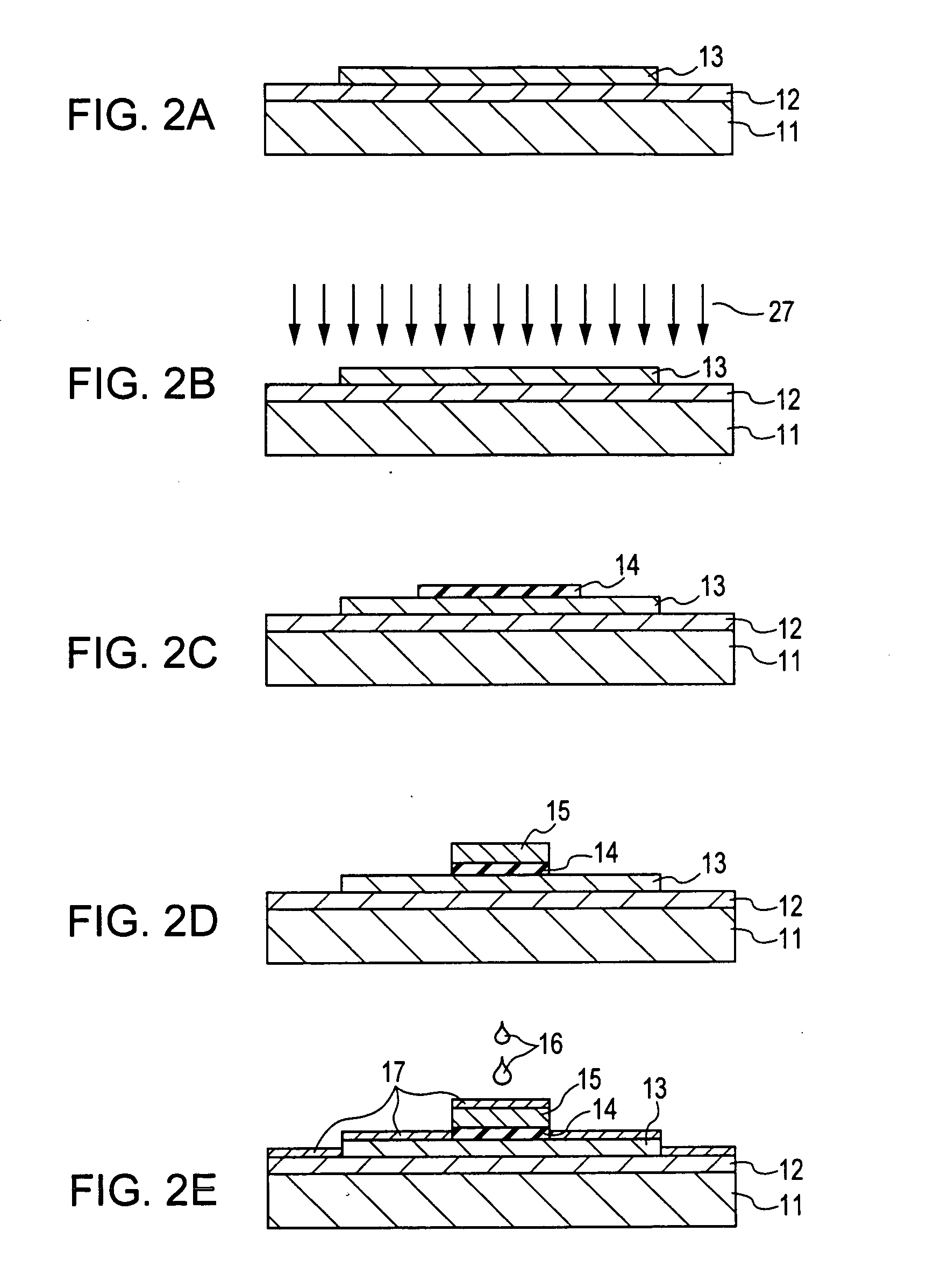
[0068]FIGS. 2A to 2E and FIGS. 3A to 3D each show a method for producing a silicon TFT according to Example 1 of the present invention.

[0069] As shown in FIG. 2A, a buffer layer 12 is formed on a substrate 11, and then a silicon film 13 having a predetermined shape and being composed of amorphous silicon or microcrystalline silicon is formed on the buffer layer 12.

[0070] As shown in FIG. 2B, the silicon film 13 is irradiated with an energy beam 27, such as a laser beam, so as to be crystallized.

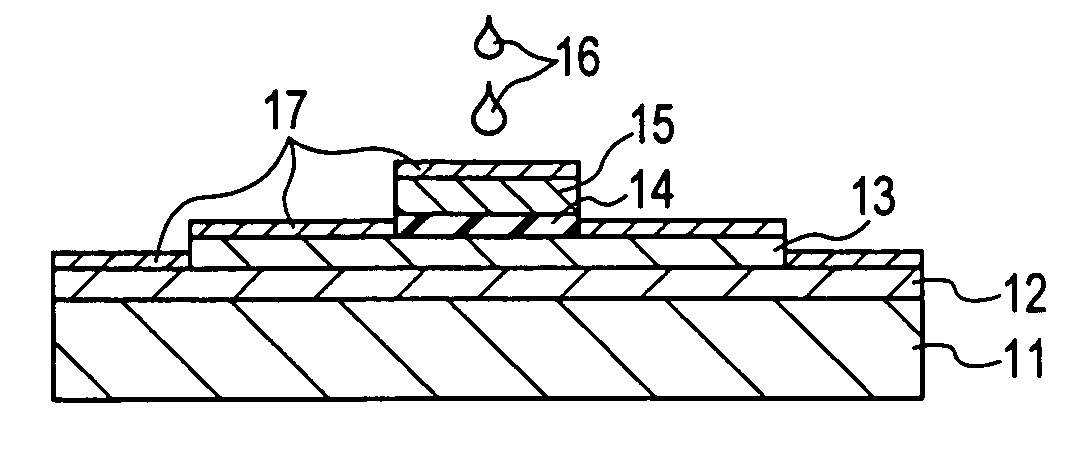
[0071] As shown in FIG. 2C, a gate insulating film 14 is formed over the surfaces of the films provided on the substrate 11. Then, the resulting gate insulating film 14 is etched so as to have a shape slightly wider than an ultimate shape.

[0072] As shown in FIG. 2D, a layer composed of a material for a gate electrode 15 is formed on the gate insulating film 14. Then, the layer is etched so as to have a predetermined pattern, thus forming the gate electrode 15. The gate insulating film 14 ...

example 2

[0078] As shown in FIG. 4A, the film forming is performed to the step of forming a silicon film 13 having a predetermined shape as in Example 1.

[0079] As shown in FIG. 4B, a gate insulating film 14 is formed as in Example 1 so as to have a shape slightly wider than an ultimate shape.

[0080] As shown in FIG. 4C, a gate electrode 15 is formed on the gate insulating film 14 as in Example 1.

[0081] As shown in FIG. 4D, a solution layer 17 containing impurity ions is formed over, for example, the surface of the silicon film 13 as in Example 1.

[0082] Subsequently, film formation is performed from the step of drying the solution layer 17 into a compound layer 18 through the step of forming a contact plug 30 as in Example 1.

example 3

[0083]FIG. 5 is a cross-sectional view showing an example of a structure of an active-matrix liquid crystal display including a switching transistor in each pixel, the switching transistor being formed by the method for producing a silicon TFT according to Example 1.

[0084] As shown in FIG. 5, a buffer layer 12 is formed on a substrate 11 composed of transparent glass or a transparent plastic. Then, silicon TFTs 31 functioning as the switching transistors are formed with a two-dimensional array by the method according to Examples 1 or 2.

[0085] A transparent electrode 32 composed of, for example, indium-tin oxide (ITO) is formed on an interlayer insulating film 28. The transparent electrode 32 is connected to the drain electrode 26 in the silicon TFT 31.

[0086] The substrate 11 having the transparent electrode 32 is disposed so as to be remote from a transparent substrate 33 having a transparent electrode 34 and a color filter 35 provided on the transparent electrode 34. The gap bet...


PUM


Abstract

A solution containing impurity ions is applied onto the surface of a silicon film to form a solution layer, followed by drying into a compound layer containing the impurities. Heat treatment is performed by irradiation with an energy beam so as to diffuse the impurity atoms in the compound layer toward the silicon film into a source region and a drain region. Subsequently, the compound layer is removed.

Description

BACKGROUND OF THE INVENTION [0001] 1. Field of the Invention [0002] The present invention relates to a method for doping impurities, methods for producing a semiconductor device and an applied electronic apparatus. For example, the present invention is suitably applied to the production of a thin-film semiconductor element. [0003] 2. Description of the Related Art [0004] Input / output devices become dramatically important with the progress of an advanced information age, and such devices are required to have greater functionality. Furthermore, in accordance with the remarkable widespread use of mobile devices in recent years, the development of a technique for forming a thin-film transistor (TFT) on a plastic substrate has been desired, the plastic substrate having advantages in that it is light, flexible, and nonfragile, compared with a general glass substrate. In such circumstances, the research and development of, for example, an active-matrix liquid crystal display (AMLCD) and a ...

Claims


Application Information

Patent Timeline
IPC IPC(8): H01L21/225H01L21/20H01L21/22H01L21/336H01L21/38H01L21/77H01L29/786
CPCH01L29/66757H01L27/1292H01L29/78618E02D5/28E02D5/76E02D17/04E02D2600/20E02D2600/30
Inventor MACHIDA, AKIOKAMEI, TAKAHIROKAWANA, YOSHIYUKI
Owner SONY CORP
Why Eureka
Try Eureka